This thread has been locked.

If you have a related question, please click the "Ask a related question" button in the top right corner. The newly created question will be automatically linked to this question.

BOOSTXL-DRV8305EVM: BOOSTXL-DRV8305EVM AVDD Error And Fault Gate Signal

Part Number: BOOSTXL-DRV8305EVM
Other Parts Discussed in Thread: DRV8305, LAUNCHXL-F28379D,

BOOSTXL-DRV8305EVM I had this product produced myself by sharing the same gerber file with the manufacturer in order to be cost effective. I used the same components on Boomlist. I made the string myself and started doing my tests. Since I have a voltage regulator in the string of the product, I did not string the LMR16006XDDC IC and peripherals. I am trying to get the product up over LAUNCHXL-F28379D. I started working by supplying Vreg voltage through Launchpad (3.3V). After powering the product from the PVDD line, I started to work on the booster I placed on the Launchpad. After energizing the booster, I observed that the LED on the nFault pin went to High as expected in the first boot. After setting the DRV8305 to the EN_Gate pin high, the nFault LED was still High. Later, I communicated with DRV8305 via SPI, cleared the error messages and read the error messages. nFault LED did not change the High state. The error messages I received are register 1 >> 0x0400 and register 3 >> 0x0020 at the following register addresses.
I sent Logic high to the PWMHA and PWMLB pins of the DRV8305 to open and control Mosfets' Gate gates, I sent logic Low to the other PWM lines. During this time, Wake and PWRGD pins were empty in case of nFault pin input in En_gate High state. Logic high GH_C High went to GH_A from the gateway I expected. When I wanted to open one of the mosfets on the low side, the next mosfet on the high side opened constantly. When I sent mosfete high on the two high side, the commands I sent went where they needed to go.
I have two questions:
1- Why do I keep getting the same errors over Nfault and over SPI even though I have communicated with SPI and deleted the errors and activated En_gate?
2- Why does a simple BLDC commutation command that I sent while the error was continuing not open the doors in the right places? Why should the low side mosfets be opened, but two high side mosfets open at the same time?
Finally, I gave the Vreg (3.3V) voltage from an external regulator and encountered the same problems. I did a DC reading from the VSENPVDD line to check if there was a problem while arraying the DRV8305 and ADC data was coming. Could you please help me
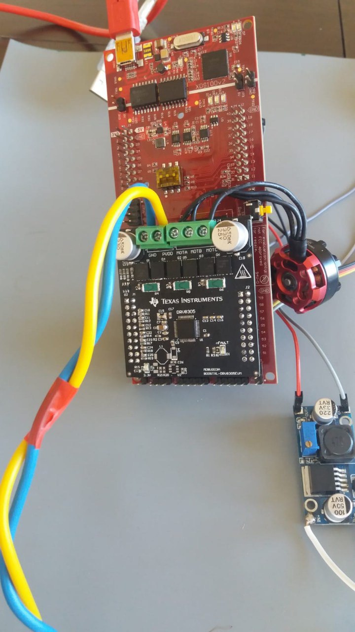
  on this subject?

  • I use DRV8305NEPHPRQ1 your products

  • Hi Mucahit,

    I understand that you did not install the 3.3V regulator to this EVM. Are there any other components from the BOOSTXL-DRV8305EVM that were left unpopulated?

    Can you send some scope captures of the gates in the scenario you described in question 2? I would like to better understand what you are seeing versus the expected output. Also, could you tell me which inputs are high and low during each capture of this scenario?

    Best regards,
    Omar

  • No I just did not array the LMR16006XDDC peripherals and itself. Logically, when I send 1 0 0 1 0 0 from the pwm lines that will go to the PWMHA PWMLA PWMHB PWMLB PWMHC PWMLC MCU outputs, namely DRV8305, the signals that DRV will send to the gates of the mosfets are as follows: 1 0 0 0 1 0 as if due to AVDD error on the hardware. The mosfet on the low side does not let the energy flow over the mosfet in the low side and the high side mosfet shifts to the next phase and opens the high side mosfet. I also see 0V in the capacitor connected from AVDD to a 1uF capacitor. 5V shouldn't come? We sent PWM at 25kHz frequency without DRV8305 solving the problem. I could not observe any PWM inputs at the inputs of the gates. I am currently providing Vreg voltage on Launchpad in our tests. What is the solution to this problem?

  • Hi Mucahit,

    The error code descriptions that you are seeing from reading SPI are as follows:
    Register 0x1: Fault Indication (0x0400)
    Register 0x3: AVDD under voltage fault (0x0020)

    To answer your question about AVDD: Yes, if the part is on there should be 5V across the 1uF AVDD capacitor  this explains the fault you are seeing. Also, can you check for 3.3V across the DVDD capacitor? Out of curiosity, how are you supplying PVDD? If you are using a power supply, how did you configure its compliance?

    Lastly, which capacitors did you install for C8 and C15?

    Thanks,
    Omar 

  • I placed the C8 and C15 schematic discharges. I am giving the PVDD a lab type control power supply. I observe 3.3V on DVDD, no problem. 5V was not coming to AVDD. The test I did yesterday would not get wet with solder on the PAD where the GND pin of the C9 capacitor will be placed. I also pulled the R7 resistance to 180 ohms. The following information is shared in the datasheet. I thought that I damaged the regulator in it and replaced it with a new one and soldered the GND side of the c9 capacitor to the PAD. For exactly why did he see it? I suspect the information.

    Thanks,

    Regards

  • Hi Mucahit,

    I am still suspicious about the capacitor to ground connection on the AVDD pin. With the board unpowered, can you measure the impedance from AVDD to GND?

    Thanks,
    Omar

  • I'm measuring 511K

  • Hi Huseyin,

    Have you attempted to re-solder C1 and retest? AVDD having a bad connection to ground would definitely cause issues. Did this board come partially assembled, or did you have to place all the surface mount components? Additionally, you could have issues if C9 or even the ground pad on the bottom of the DRV8305 is making bad contact.

    Best regards,
    Omar

  • Hi Team

    First of all, I changed the capacitor C1. The problem was not solved and continued. Then I noticed that the C9 capacitor had cold solder on the GND side. It was touching the leg of the capacitor to the GND side. But it was not soldered. I arranged all the components myself. I solved the problem by replacing a new DRV8305 and re-soldering the capacitor C9. I was wondering if this C9 cap was not connected with GND, so could current flow from Vreg pin to LDO regulator? Can I run the DRV8305 that I changed from the board if I solder it to another board?

  • Hello Huseyin,

    I just wanted to let you know that responses will be delayed as a result of the holiday in the US this week.

    We'll make sure we respond no later than 12/4/20.

    For some intro info on VREG, usually the output caps for the regulators help maintain stability of the output. In addition, VREG also supplies power rails within the part for various digital logic circuitry so if the output of the regulator was unstable and could not accurately sustain the voltage or charge required internal to the part, you should expect to see the same problems.

    Thanks,

    -Cole

  • Hi Huseyin,

    To echo what Cole mentioned, the VREG output cap having poor connection to ground very well could have caused instability in the regulator and subsequently issues sustaining the voltage internal to the part.

    As for the malfunctioning DRV8305, I do not have sufficient information to determine whether or not the driver was damaged during operation when the capacitor was making poor contact. It may be worth testing, but I would be sure the assembly of the new board does not have any issues to rule that out in case the part did get damaged. I would not recommend using this part in any end products and testing it on another board would be strictly for debug. 

    Just to confirm, the original problem was solved when you replaced the DRV8305 and re-soldered C9?

    Best regards,
    Omar

  • Thank you for your answer yes. I replaced the DRV8305 and re-soldered the GND leg of the C9 Cap. Problem solved. If it has not been met with such an error before, if there is a need for any test results, we will not be able to know if the problem is actually occurring for this reason. You can close this topic then.