This thread has been locked.

If you have a related question, please click the "Ask a related question" button in the top right corner. The newly created question will be automatically linked to this question.

DRV8353: SRM motor control with hall sensor

Part Number: DRV8353
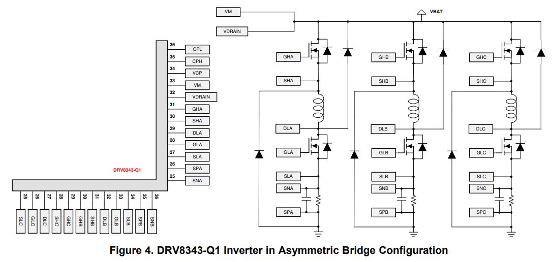
Other Parts Discussed in Thread: DRV8343-Q1

Hi,

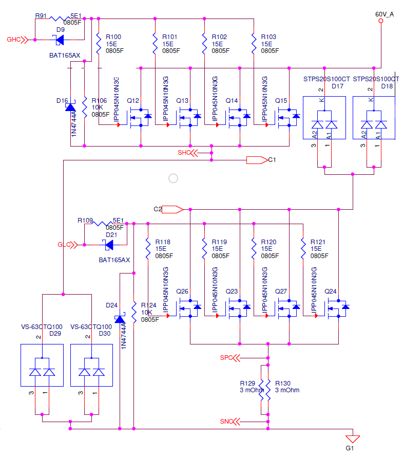
I am using drv8353 and delfino for controlling 3 phase SRM motor with hall sensor feedback for position measurement. I am able to rotate the motor in no load. In load the over current fault occurs even with low load. In no load also, the 3 phase currents are not equal. Anyone having experience with SRM motor control, kindly help me to solve this problem.

Note: feedback - magnet disc is attached with shaft and hall sensor is placed against it.

  • Hello Kaarthi,

    We like to refer to this app note to discuss SRM motor circuits. Are you implementing an asynchronous or miller bridge configuration (figures 4 and 5 from the linked app note)? Or some other configuration? Can I see your schematic?

    On the DRV8353, overcurrent will be tripped by a few things. Are you using a SPI device where you can read the fault bits being set for diagnostics?

    • High-side MOSFET overcurrent: Measured from VDRAIN to SHx - if this voltage increases beyond the VDS threshold when the MOSFET is turned ON, it will trigger an overcurrent fault.
    • Low-side MOSFET overcurrent: Measured from SHx to SPx - if this voltage increases beyond the VDS threshold when the MOSFET is turned ON, it will trigger an overcurrent fault.
    • Sense amplifier overcurrent: Measured from SPx to SNx - if this voltage increases beyond the SEN_OCP threshold, it will trigger an overcurrent fault.

    Thanks,

    Matt

  • Hi,

    1) I am using asynchronous bridge configuration.

    2) I am using DRV8353 Hardware config so, no spi communication possible.

    Do you any hall sensor based SRM control reference design or any application note or any source code?

    Thanks,

    Kaarthi

  • Hello Kaarthi,

    How is SHx connected in the circuit? If it is on the top or bottom of the load then overcurrent fault will trip because VDRAIN-SHx or SHx-SPx will be > VDS threshold.

    Can you disable the overcurrent VDS monitor (tie the VDS pin to DVDD) to see if the issue goes away?

    I do not think we have any SRM control reference design or code that is available. The app note linked above (LINK) is the only content that I could find.

    Thanks,

    Matt

  • Hi,

    Can you disable the overcurrent VDS monitor (tie the VDS pin to DVDD) to see if the issue goes away?

    The VDS is already tied to DVDD.

    I do not think we have any SRM control reference design or code that is available. The app note linked above (LINK) is the only content that I could find.

    Any proven articles also be helpful....

    Refer the schematic attached.

    Thanks,

    kaarthi

  • Hi Kaarthi,

    Thanks for sharing the schematic!

    I see that the MODE pin is configured to be 6x PWM (MODE tied to GND). I think for proper SRM operation you need to use the independent PWM mode (MODE pin tied to DVDD) so that the high-side and low-side MOSFETS can be on at the same time. In 6x PWM mode the high-side and low-side FETs in the same 1/2-H bridge cannot be on simultaneously.

    nFAULT can pull low because of a few different faults which we can diagnose:

    • VM or VDRAIN undervoltage (ensure VM > 9V & VDRAIN > 7V)
    •  Charge pump undervoltage (measure VCP to ensure the voltage is around VDRAIN + 11V)
    • VGLS regulator undervoltage (measure VCP to ensure the voltage is around 11V)
    • VDS overcurrent (this fault is disabled in your schematic)
    • Sense overcurrent (SPx needs to exceed 1V for this fault to trip, it will automatically retry after 8 ms and you will see a pulse waveform on nFAULT)
    • Gate driver fault (MOSFET was not able to turn ON or turn OFF within 4us)
    • Thermal shutdown (IC temperature too hot)

    SRM documents/articles:

    • This is a much older app note related to SRM drive: LINK
    • SRM motor position estimation: LINK
    • Control using DRV8343-Q1: LINK
    • Motor Control Compendium (page 71): LINK
    • Switched Reluctance Motor Control – Basic Operation and Example Using the TMS320F240 (attached to post) - spra420a.pdf

    Thanks,

    Matt

  • Hello Kaarthi,

    I can see that you clicked "This did NOT resolve my issue."

    Do you have any comment based on my post above?

    Thanks,

    Matt

  • Hi Matt,

    I really thankyou for the documents you provided. It will help us a lot. 

    While observing the PWM signals of the phase in which we had a lesser current, we found that the PWM signal is turned OFF before the actual turn OFF time.

    For the 8% given duty in 14khz, the expected turn ON time is 5.6us, but the actual turn ON time is as shown in the figure as 4.6us. 

    The signal is captured at the output of gate driver and at the input of gate driver the turn ON time is 5.6us.

    To verify these signal we removed the gate resistor also, still getting same problem. 

    And when the duty increases like 30% at gate driver input, we are getting only 15% duty on output.

    Note: In the other two phases, the duty is OKAY. 

  • Hello Kaarthi,

    When the duty cycle truncation happens, does the nFAULT pin pull low? Can you capture nFAULT, INHx, GHx, and SHx on the same oscilloscope screen to see the behavior? If nFAULT is toggling then you are hitting over current, either the sense amplifier over current or VDS over current.

    In 6x, 3x, or 1x PWM, I would expect the output PWM duty cycle to be reduced by the dead time (1 us typical). In independent PWM mode the dead time is not inserted.

    Which channel is this occurring on, and is there any schematic or layout difference between this channel and other channels?

    Thanks,

    Matt

  • Hi Matt,

    When the duty cycle truncation happens, does the nFAULT pin pull low? Can you capture nFAULT, INHx, GHx, and SHx on the same oscilloscope screen to see the behavior? If nFAULT is toggling then you are hitting over current, either the sense amplifier over current or VDS over current.

                     No, nfault doesn't occur.

    In 6x, 3x, or 1x PWM, I would expect the output PWM duty cycle to be reduced by the dead time (1 us typical). In independent PWM mode the dead time is not inserted.

                    I'm using independent pwm mode

    Which channel is this occurring on, and is there any schematic or layout difference between this channel and other channels?

                    This is occurring only in phase A. Schematic wise, all are same. Only thing is, in layout wise phase A MOSFETs are little bit far when compared to other phases from gate driver.

    This duty cycle truncation happening even when the motor is not connected.

    Regards,

    Kaarthi

  • Hi Kaarthi,

    Can you capture a few different waveform for me to get a better idea what is going on?

    • INHx, GHx, SHx, and GLx on Phase A (looking at two different duty cycles) and Phase B 
    • INLx, GHx, SHx, and GLx on Phase A (looking at two different duty cycles) and Phase B
    • GHx, SHx, and VDRAIN on Phase A (measure VDRAIN directly at pin 4)
    • SHx, GLx, SPx, and SNx on Phase A

    Thanks,

    Matt

  • Hi matt, 

    Please find the below captured waveforms,

    1) AT,GHA,SHA,GLA,8%- duty

    2) AT,GHA,SHA,GLA,15%- duty

    3) BT,GHB,SHB,GL,8%- duty

    4) BT,GHB,SHB,GL,15%- duty

    4) GHA, SHA, VDRAIN,15%- duty

    NOTE: I am using the soft switching as bottom switches is complete high for respective phase sequence.

    Thanks,

    kaarthi

  • Hi Kaarthi,

    You have a very small voltage scale, so it is difficult to be sure, but it looks like phase A is not being fully enhanced on the high-side MOSFET. From your last waveform SHA is ~48V while GHA is also around 48V. On phase B (waveform #4), SHB is ~48V while GHB is closer to ~58V as expected. As I mentioned, it is hard to make out from this scale.

    Can you take waveforms #3 and #4 again with a different voltage scale? Can you overlay GHx and SHx on the same plot with 5V/div or less for channels A and B?

    Please confirm that the gate-to-source zener on phase A is not broken (the equivalent of D16 on phase C), as this could be clamping the voltage.I noticed that this component has a non-repetitive peak reverse current limit of 300mA which is much lower than the gate drive current.

    Thanks,

    Matt

  • Hi matt,

    Please look at the attachment of phase A and phase B showing GHx and Shx, The waveforms taken at 8v/div.

    1) Phase A - Green - GHA, Pink - SHA,

    2) Phase B - Green - GHB, Pink - SHB

    From the above waveforms, we can clearly see that the gate voltage amplitude is completely different from faulty phase and working phase.

    We checked even by removing that VGS zener diode on all phases, this results same.

    One more thing we noticed is, on the faulty phase the VGS resistor showing 45 ohm only actually it is 10kohm. On other phases it is showing 10k(including bottom of phase A) . We removed the resistor and checked the same , it is showing 10k.

    Regards, 

    kaarthi

  • Hello Kaarthi,

    It is possible that the high-side gate of phase A can be damaged on this IC. Have you tried replacing the DRV8353H with a new IC to check if the operation is as expected?

    When you remove the DRV8353 IC, can you do a curve trace on the GHA and GHB nets (while the DRV8353 is off the board). Use a power supply with a 10mA current limit and vary the applied voltage from -2V to 11V in 0.5V increments (applied from GHx to SHx). Make sure the system is powered OFF when you do this.

    Have you tried operation after removing the 10k resistor? There could be a solder bridge under the component on the board causing a 45 ohm short. There could be a solder bridge located somewhere else on the board as well pulling down the GHA node.

    Thanks,

    Matt

  • Hi Matt,

    We tried of replacing gate driver ic's of 14 nos on 4 different boards, no answer we got...

    Yes, we can do the curve trace but I don't know how it helps.

    We tried to operate with that 10k resistor still results are same.

    Regards,

    Kaarthi

  • Hi Kaarthi,

    The purpose of the curve trace test while the device is off of the board is to check for board-level shorts on the MOSFET gate. When you mentioned that the gate-to-source resistor measured 45 ohms on board but 10k off board, this would indicate to me that there is a parallel 45 ohm path on the board, occurring inside or outside of DRV8353. By removing the DRV8353 from the board we can isolate the potential on-board short and the curve trace will help us identify if any issue is present.

    Since you mention that replacing the DRV8353 results in the same issue, this points me towards a low-impedance path on the board. The failure seems to follow the board, not the part.

    Thanks,

    Matt

  • Hi Matt,

    Once we removed the 10k resistor, still it was showing 45 ohms with gate driver on board. So, we removed the gate driver, then its not showing 45 ohms.

    We also did curve trace as you suggested in your previous post. We gave from GHx to SHx, it seems ok. Find the following pictures,

    1) Applied voltage - 0.6V, Scope scale - 1v/div

    2) Applied voltage - 3.0V, Scope scale - 1v/div

    3) Applied voltage - 6.8V, Scope scale - 2v/div

    Regards,

    Kaarthi

  • Hi Kaarthi,

    I have some concerns with your measurement methodology. I will send you a friend request over the E2E system so we can discuss in more detail.

    Thanks,

    Matt

  • Hi Matt,

    I don't think, the measurement methodology is wrong, because I applying voltage on only one track in the whole board and the voltage is coming out without any drop on MOSFETs pins. How can you say the measurement methodology is wrong. Please tell me what's wrong.

    Regards,

    Kaarthi

  • Hello Kaarthi,

    Please check your notifications (top right of the page when you are logged in). Can you accept my friend request so that we can chat over private message?

    Thanks,

    Matt

  • Closing this thread since the discussion was taken off-line.

  • To close out this thread after offline discussion:

    It is clear that the charge pump (VCP) is not damaged, which aligns with our assumed root cause: damage to the high-side gate driver sink


    Turn off test is eeded to check if there is a significant voltage spike on SHx: Measure SHx, GHx, GLx, and load current on an oscilioscope. Turn on GLx and afterwards turn on GHx to let large current flow through the load. After a little bit of time, turn off GHx. Trigger scope capture on falling SHx waveform and zoom into 100-500ns so we can check for any significant negative voltage spikes at SHx.


    My theory is that the clamping diodes (i.e. D29, D30) are too slow to catch and cause negative voltage spikes to occur on SHx when the high-side MOSFET turns OFF. You may want to look for a faster diode (maybe not a Schottky) to use. Alternatively, you may need to add capacitors on SHx to GND to help absorb some of the energy.


    Thanks,

    Matt