This thread has been locked.

If you have a related question, please click the "Ask a related question" button in the top right corner. The newly created question will be automatically linked to this question.

DC coupling DRV8662EVM

Other Parts Discussed in Thread: DRV8662

Hi,

I have an application that requires DC coupling. Can I DC-couple the inputs by removing the filter capacitors C4 and C5? I'm assuming this would be ok providing that the inputs are driven differentially with a bias of say 2V (for a 200V range and 40dB gain.)

Thanks,
Andrew

  • Andrew,

    There are a few issues with DC coupling, but it is possible.

    1. The offset voltage of the DRV8662 could change with and without the capacitors (up to ~1V change)
    2. The common-mode of the DRV8662 is VDD/2, so there will be some current exchanged with the source ( VDD/2 - VCM[source] ) / 100k
    3. With such a high gain any DC offset can have a large impact on the output signal.

    Thanks,
    Brian

  • Brian,

    I picked up the EVM for driving a PZT (Piezoelectric Cylinder for applying DC to frequency determined by cutoff of the amplifier for controlling Mach Zehnder Interferometer with fiberoptics attached it to compress and stretch fiber to compensate for environemental effects) but not Piezo Haptic applicaitons.  Unlike Andrew's application requiring high gain across the band, I would like to use it in the lowest gain mode but constant gain from DC to Cutoff.  So far, I've done the following described in the EVM Manual:

    1.  Replace resistors R6, R7, R13 adn R14 with 0-Ohm resistors.

    2.  Remove resistors R17 and R18.

    3.  Remove capacitors C8, C9, C13 and C14.  Do not remove AC coupling capacitors C4 and C5.

    Do I further have to do what Andrew did or can I use it as is for DC operation (does the capacitor form a divider network at DC and have response or would there be a DC offset issue)?

    Look forward to your response.

    Thank you!

    Peter Ranon


  • Hi Peter, you're on the right track to DC couple the amplifier. Be aware that this method requires a differential input signal that is biased around Vsupply/2, which can be rather annoying if you're not driving it from a DAC. I have designed a piezo driver board based on the DRV8662 that might assist you. In particular, this board contains a level shifting stage that accepts an input referenced to ground making it easier to use in applications like ours. Let me know if you need any further details.

    http://www.piezodrive.com/products.html#pdu100b


    Regards,

    Andrew

  • Andrew,

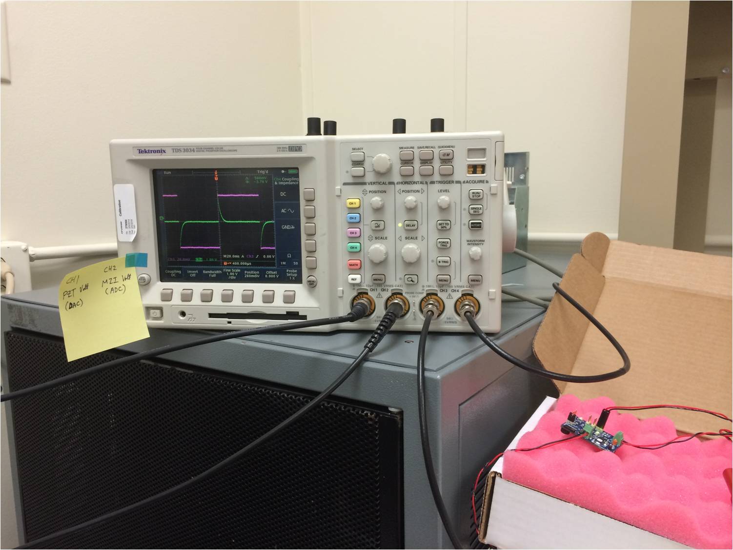
    Thank you for the feedback.  I got High Pass Filter response (oscillocope photo with input in purple and output in green) with with C4 and C5 left in the circuit. 

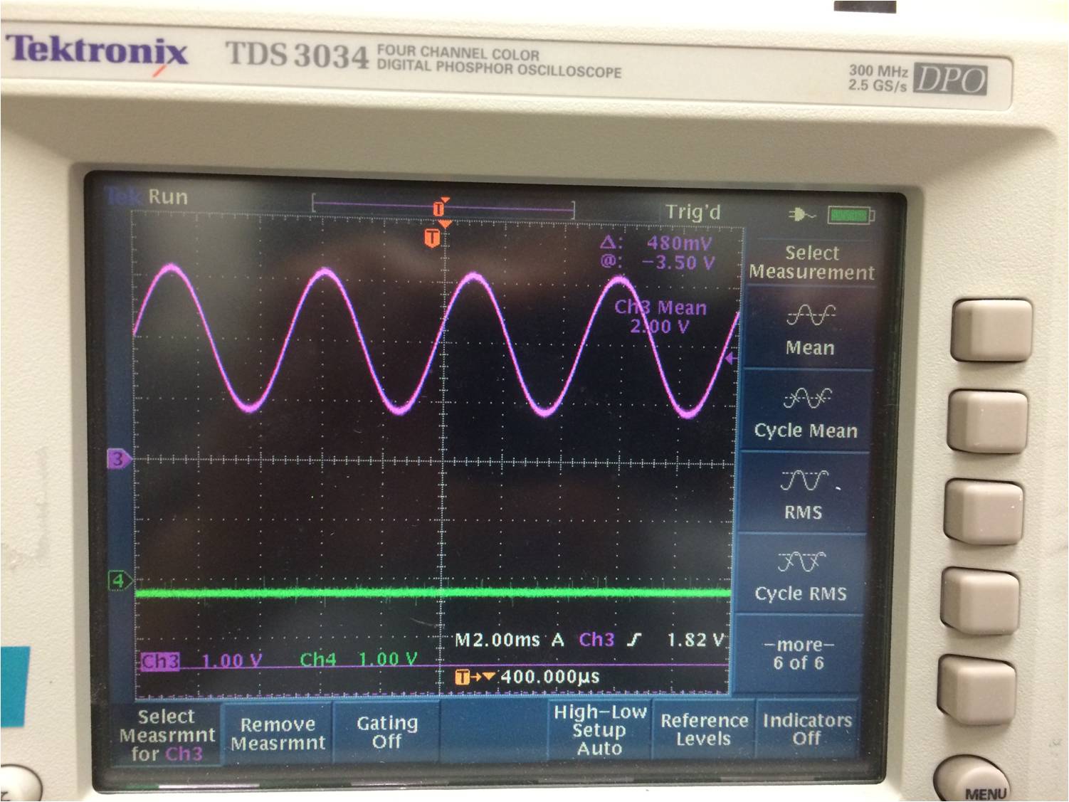
    So I removed C4 and C5 then set Vsupply = +4.00V then added Vsupply/2 = +2.00V (see "mean" for purple trace) to the Input (so my input is now +2.00 + AC):

    Then tested through 4 sets of gain settings (00, 01, 10, 11) and adjusted input with DC offset of +2.00V +/-0.5V or +1.50V to +2.50V (i.e., in vicinity of Vsupply/2) and swept through input waveform from 6Hz to 200Hz but the output remained at DC offset (same as 3rd photo).  Should I put back C4 and C5 to repeat the High Pass Filter test (to get the same as 1st photo) to make sure I have not broken the PWB?

    I looked through the link you provided but I was unable to determine which device would have DC response.  They all appeared very similar to the EVM I currently have.  Please let me know the logical next step.  Thank you!


    Best,

    Peter Ranon


  • Your circuit seems correct, are you sure the scope isn't AC coupled?

    The other boards I mentioned are all DC coupled.

    Regards,

    Andrew

  • The circuit is DC coupled  to the oscilloscope - you can see the DC offset with both the CH3 input (purple with +2.00V from the CH3 0V reference point) and CH4 output (green with slight offset from the CH4 0V reference point) and you wouldn't see steady DC when AC coupled so I have that covered but wanted to ask about your C4 and C5.  I initially had them when I got the HPF reponse (looks like a derivative) but went ahead and removed them and replaced them with a 0-Ohm.  Do you have C4 and C5 in your circuit?  If you do, I need to put them back in then apply input with Vdd/2 offset.  Thank you!

    Peter

  • There are no capacitors in my circuit, you should be measuring a DC response. I suspect something is damaged somewhere along the signal chain. Andrew

  • Thank you for the feedback - "I suspect something is damaged somewhere along the signal chain" - TI suggested the same thing but want to confirm - you replaced C4 & C5 with a 0-Ohm short to the input of U1 then applied Vdd/2 to offset the input (if Vdd = 4V, then Vdd/2 = 2V, so Vinput = Vdd/2 + Signal (AC), correct?  How critical was the Vdd/2 offset?  Did it come out exact or were there internal imbalances that kept it slightly off of Vdd/2?  I hunted around a bit around Vdd/2 but didn't see it jump from - to +, it just latched down at - (negative offset).

    With DC coupled input with Vdd/2 offset, your max input is 1/2 correct?  I don't think it matters much in your case since you have large gain and the AC swing amplitude of Vdd/2 (with offset, +Vdd to 0) is more than enough swing at the output, right?  Did you try sweeping the frequency response with such high gain?  Did it obey Gain*Bandwidth Product Rule for the 1st corner (aka cutoff) frequency?  Did you measure the Fc for the various gain values?

    Peter