This thread has been locked.

If you have a related question, please click the "Ask a related question" button in the top right corner. The newly created question will be automatically linked to this question.

DRV8323R: The chip drives a three-phase motor, and the motor speed cannot go up

Part Number: DRV8323R
Other Parts Discussed in Thread: DRV8323

Hi Team,

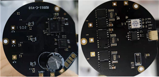
The customer used DRV8323RH to drive the motor. The target motor with blades can reach more than 5000 rpm, but actually it can’t go up to 4600 rpm. The external power supply is 20V, about 18A.

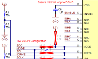
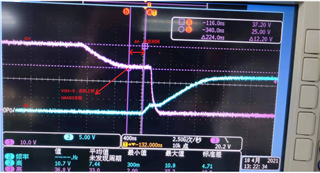
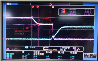
He changed the gain from 10 times to 5 times (the gain pin pulls down the 45.3K resistance into the ground to directly ground) . The customer assumes that the gain is doubled, and the current of each phase of the three-phase motor should also be doubled. However, it is actually measured that the maximum speed of the motor with blades can only reach 4800 rpm. At this time, the external power supply is 20V/20A.

DRV8323RH DESIGN.pdf

Customer would like to know how to resolve this case?

Thanks,

Annie

  • Hi Annie,

    I will review the schematic today and leave feedback by the end of the day.

    In the meantime, is the customer running the motor unloaded? What frequency is the customer running the PWMs?

    The Gain setting of the Current Sense Amplifier is used to amplify the shunt resistor voltage to the SOB voltage from its VREF value. So in bidirectional mode, it is VREF/2 - VSOx. The gain allows the customer to have a trade-off: a larger gain setting allows for more resolution in current measurement, and a lower gain setting allows for more range in current measurement. However, changing the gain will double the current reading in software, this will not physically change the current going through the motor because that is entirely dependent on the motor itself and how the motor is being commutated, i.e. PWM frequency, control method, position feedback.

    From a quick glance at the schematic, it looks like the customer is running sensorless trapezoidal firmware since the customer is detecting the position of the motor through monitoring the phase currents. Can you confirm if this correct? 

  • Hi Aaron,

    The customer used a paddle. The PWM frequency of the governor is 20khz. He previously suspected that the output values of SOA, SOB, and SOC exceeded the sampling range of the MCU ADC (0~3.3V), which caused the speed to reach 4800 rpm and could not be pushed up. So he adjusted the gain from 10 times to 5 times. But it may not actually be because of this problem. 

    Would you possible to check is there any other reason?

    Thanks,

    Annie

  • Hi Annie,

    Speed is controlled generally by the voltage, so can the input voltage be raised to reach the 5000 rpm requirement?

    Can you confirm how the customer is measuring the RPM? Is it being measured in software or with an instrument?

    If calculating the speed in software, the customer needs to ensure that the motor parameters entered in software are correct to calculate the speed correctly. This E2E post may be helpful: https://e2e.ti.com/support/motor-drivers/f/motor-drivers-forum/746216/drv8303evm-maximum-speed-limit

    Finalizing the schematic review today.

  • Hi Annie,

    Attached is my review for the schematic from the initial post. I noticed that the customer has all of the SPx/SNx connections backwards. They connected the high-side of the shunt resistor (A_x_I) to SNx rather than SPx...this will invert all of their current measurements. Attached is some other general feedback for future designs. 

    DRV8323RH DESIGN_AMB.pdf

    Please provide feedback from the previous post in terms of how customer is calculating speed in their application. 

    Thanks,
    Aaron

  • Hi Aaron,

    VBAT=20V power supply, with blades, speed adjusted to 3900 (current to about 8A)

    The customer tested the surface temperature of the NMOS tube and DRV8323RH chip on the governor board. The test lasted for an hour:

    In the first 10 minutes, the temperature of the NMOS tube will reach 90 degrees. But the temperature will slowly drop later, and it will remain at 69 degrees after more than 30 minutes.

    But the surface temperature of DRV8323R reached 120 degrees after 10 minutes. Later, the voltage was adjusted to 23V for power supply. After 5 minutes, the surface temperature of DRV8323RH reached 145 degrees. 

    Would you possible to share your suggestion for resolving the case?

    Thanks,

    Annie

  • Hi Annie,

    Can you remind me if this is on a custom board? If so, can you share the layout?

    A typical cause of DRV8323 overheating is having minimal thermal vias for the DRV8323 and having the PowerPad not having great thermal escape.

    The threads below may help:

    https://e2e.ti.com/support/motor-drivers/f/motor-drivers-forum/855228/drv8323-overheating

    https://e2e.ti.com/support/motor-drivers/f/motor-drivers-forum/784030/drv8323-drv8323h-driver-chip-overheating-abnormally

  • Hi Aaron,

    ESC.brd

    PWM frequency is 20khz. He uses the board he made. DRV8323RH thermal pad has a lot of heat dissipation holes. Please refer to the attachment above for pcb layout. 

    Thanks,

    Annie

  • Hi Annie,

    Thank you for sharing layout. Few more questions:

    How many layers is the PCB? We recommend a 4-layer PCB to dissipate heat from the thermal pad on the DRV device to an inner ground layer inside the PCB using direct-connect vias. 

    Are you applying any external load on DVDD other than what is in the schematic? The largest thermal loss in the DRV devices is current load on the LDO as the power dissipated would be the voltage difference times the current. 

    Is the customer applying PWM duty cycles <100%? Is there better thermal performance when running at 100% PWM duty cycle?

    Thanks,
    Aaron

  • How many layers is the PCB? We recommend a 4-layer PCB to dissipate heat from the thermal pad on the DRV device to an inner ground layer inside the PCB using direct-connect vias. 

    layers . you are able to refer ESC.brd

    Are you applying any external load on DVDD other than what is in the schematic? The largest thermal loss in the DRV devices is current load on the LDO as the power dissipated would be the voltage difference times the current. 

    It isn't any external load on DVDD other than what is in the schematic

    Is the customer applying PWM duty cycles <100%? Is there better thermal performance when running at 100% PWM duty cycle?

    PWM duty cycle is variable. The maximum PWM duty cycle he set is about 90%. (Because of dead time and other reasons)

    Thanks,

    Annie

  • Hi Annie, 

    Thanks for the replies. 


    I also just noticed on the schematic that the IDRIVE pin is tied to DVDD. This results in 1-A/2-A source/sink gate drive current and can lead to unintended behavior at the DRV and MOSFETs. The MOSFETs used in the design have Qgd = 29nC, resulting in switching waveforms at rise and fall times of 29nC/1A = 29ns and 29/2A = 14.5ns. These are extremely fast switching events that will more than likely reduce the longevity of the gate driver and MOSFETs due to voltage ringing, cross-conduction, and potential dV/dt coupling into the gates if the layout is not optimized enough to handle the fast switching from the large IDRIVE current. 

    It is recommend on layouts for Hardware variants of the device to at least have a resistor divider at the Hardware pin so that the appropriate resistor can be populated to evaluate different settings, i.e. IDRIVE, VDS, etc. 

    I would recommend seeing if the customer can find a way to try to evaulate the following settings to see if the DRV performance improves and reduces overheating at the device:

    - Tying the IDRIVE pin to GND (10mA/20mA source and sink current)

    - Floating the IDRIVE pin (120mA/240mA source and sink current) 

    Is ESC.brd supposed to be a working link to the layout? It only appears as text.

    Does the device operate at a lower temperature at a smaller supply voltage, i.e. 12V? 

    Thanks,
    Aaron

  • Hi Aaron,

    1. In the next revision, he will add pull-up resistors and pull-down resistors at IDRIVE and VDC. In the reference design, the pull-up and pull-down are all 75K. How much is the partial pressure here? Is there a standard?

    2. He also attached layout, please help to review it ESC.rar

    3. When the customer was debugging the governor, he found that the Miller platform lasted a long time (about 600ns) when the H-side NMOS was turned off. He tried to change the NMOS with a much smaller Qgd, or adjust the resistor connected in the Gate terminal, but it didn’t work. He suspected that it was a problem with the driver chip DRV8323RH. Is it related to excessive IDRIVE current? Or are there any other factors?

    Thanks,

    Annie

  • Hi Annie,

    1. IDRIVE selection is essential for gate drivers because there are a lot of factors that can affect proper MOSFETs switching such as board layout, parasitic inductances and capacitances, and MOSFET gate-drain capacitance (Qgd). Therefore, our gate driver devices offer a configurable IDRIVE setting to adjust the gate drive current needed to turn on MOSFETs efficiently and prevent ringing, cross-conduction, or damage to the DRV or MOSFETs from hard switching. 

    This E2E FAQ explains more about why IDRIVE is important and how to select an IDRIVE setting based on the MOSFET's Qgd value and rise/fall time of the MOSFET VDS: https://e2e.ti.com/support/motor-drivers/f/motor-drivers-forum/796378/faq-selecting-the-best-idrive-setting-and-why-this-is-essential

    Here is an app note that describes IDRIVE in detail: https://www.ti.com/lit/slva714

    To iterate from before, switching 100ns - 200ns is generally fast rise/fall times for customers and because the customer is using the max IDRIVE setting, this will result in rise/fall times of 14.5ns - 29ns and will likely cause those unintended effects on the DRV or MOSFETs. A good practice is to start evaluating with a low IDRIVE setting and raise the setting higher if needed for faster switching to suit what is best for the customer's system. In this case, the H/W variant allows 7 configurable IDRIVE settings, so it is best for future revision of the PCB to include the resistor divider at the IDRIVE pin to allow configurable resistors tied to DVDD or GND. 

    2. I will check out the layout today and leave feedback by end of day.

    3. It is recommended to evaluate IDRIVE without using a gate resistor (or populating a 0-ohm) at first because it complicates calculating the IDRIVE setting from post #1. Adding a gate resistor will significantly reduce the gate drive current and should only be added if the IDRIVE needs to be lower than the lowest IDRIVE setting (10mA/20mA). A long Miller region indicates that there is a small amount of current (due to the gate drive resistor) to turn on the Qgd of the MOSFET. I also see that there is extra capacitance of 1nF between gate-drain of the MOSFETs, this will also significantly increase the Miller region turn-on time. 

    I would first replace the 51-ohm resistors with 0-ohm resistors, remove C41-C43 and C47-C49, and then try to tie the IDRIVE pin to GND (10mA/20mA), and see how the system performance changes. If the Miller turn-on region is still too long, then try floating the IDRIVE pin for 120mA/240mA gate drive current, and see if the waveforms improve. 

  • Hi Aaron,

    Thanks for your help.

    When customer uses IDRIVE and VDC floating to test the input of 23V/8A (4000 rpm), the temperature of the DRV8323RH chip drops significantly (the surface of the chip is 105°C). The overheating problem should be caused by this reason. After the subsequent hardware revision, he will continue to debug IDRIVE and VDC to improve.

    Please continue to review the layout to see if there is anything that needs improvement.

    Thanks,

    Annie

  • Hi Annie,

    I will need to download EAGLE to be able to open the board layout. This may take time and I'll respond on Monday at the latest since tomorrow is a holiday. If possible, can the customer save the board layout as eagle v6 XML so that it can be viewed in Altium PCB Viewer?

    Here is a forum that describes the issue: https://forums.autodesk.com/t5/eagle-forum/how-to-convert-eagle-file-to-eagle-v6-xml/td-p/7073410

    Alternatively, feel free to share screenshots of layout if possible. You may do so publicly over this forum or privately over E2E friend request.

    Glad to hear IDRIVE debug has lowered die temperature. Let us know if you have any outstanding questions.

    Thanks,
    Aaron

  • Hi Aaron,

    It is drawn using allegro, ad should be able to find your Orcad file format by clicking File→Import Wizard→Next. Would you able to find it?

    Thanks,

    Annie

  • Hi Annie,

    Friday 4/2 is a holiday in the US. Aaron will get back to you on Monday!

    Thanks,

    Matt

  • Hi Annie,

    I received the layout over email and am sending review suggestions by end of the day. May I close the thread on E2E?

  • Hi Aaron,

    The customer has a follow-up question today that needs your moderation: The problem of too long duration when the GH terminal is turned off

    He removed all the surrounding resistors and capacitors, and then adjusted IDRIVE. Figure 1 below shows the idrive connected to the ground with a 75K resistor and Figure 2 below is floating.

    The waveform tested above was tested when no load.

    His understanding is that when the upper NMOS VGS=0, the upper NMOS is turned off. Then, the time until the lower tube VGS>0 is Δt dead time. Adjusting IDRIVE can also adjust the dead time. (It can be clearly seen from the figure that when idive floating, the NMOS turn-off time becomes shorter and the dead time is longer) Does his understanding is correct?

    Why is the upper bridge NMOS VGS=0 turned off, but at this time VG=VS=VD=25V, it does not drop down immediately (this voltage dead time has been maintained), but waits until the lower bridge NMOS is turned on and the Miller time Did it fall quickly?

    Thanks,

    Annie

  • Hi Annie,

    The purple waveform is measured between the gate drive voltage and ground. (GHx-GND) The customer should measure the waveform between the gate and source (GHx-SHx) to see the relationship between the high side and low side gate drive signals. 

    Smart Gate Drive uses a state machine architecture and handshaking to ensure that the FETs switch properly. Once the high side FET turns off (VGS = 0V), dead time is inserted. In the H/W version, dead time is fixed at 100ns. Then the low side turns on with the according IDRIVE setting and at a fixed time TDRIVE for 4000ns in the H/W version. 

    When the low side turns on, the high side has a strong pulldown current (ISTRONG), which forces the high side gate voltage to 0V. So VGS = 0V on the high side when then the low side turns on, which is what is exactly happening in the waveform above. 

    Changing IDRIVE simply changes the gate drive current strength when turning on the MOSFETs. When higher gate drive currents are used, the MOSFETs have higher VDS slew rates and the increased current will decrease the VGS turn-on time and Miller region. But the dead time will remain fixed at 100ns. 

    Thanks,
    Aaron

  • Hi Aaron,

    There is also a dead time setting on the MCU. What effect will this have on the final dead time? Does he need to add dead time on the MCU side?

    GH is off, when the upper bridge NMOS VGS=0, the NMOS should be off. At this time, the lower bridge NMOS has not been opened yet. Why does the voltage of the upper bridge VG=VS=25V not drop at this time, but wait until the lower bridge NMOS is turned on before the high-side strong pull-down current drops rapidly?

    Thanks,

    Annie

  • Hi Annie,

    Dead time can should be inserted from the MCU. The DRV8323 uses VGS monitoring to check the true state of the VGS of each FET to determine if it is truly ON or OFF and inserts extra dead-time on top of the programmed value. Some IDRIVE adjustment (lower) or snubbing may be required to control the VGS tighter and therefore allow the FETS to switch quicker. 

    The DRV8323RH has fixed 100ns dead time, so even if the MCU inserts programmed dead time, the DRV8323 is checking to ensure that there is exactly 100ns of time between when the FETs are truly off (I believe VGS < 2V). 

    The customer should measure VGS of the HS MOSFET to determine exactly when the FET is off and the VGS of the LS MOSFET to determine when it turns on to see the dead time insertion since measuring gate to ground is not obvious to see when the FET is truly off. When the LS FET turns on, then ISTRONG is sunk on the HS gate to pulldown the FET to SHx, which in this case is 0V because SHx = 0V when the LS turns on. 

    Thanks,
    Aaron

  • Hi Annie,

    Is any additional help needed on this thread?

    Thanks,

    Matt

  • Hi Aaron,

    The customer did not give me any response. You are able to close this thread now. Once there is feedback, I will let you know.

    Thanks,

    Annie