This thread has been locked.

If you have a related question, please click the "Ask a related question" button in the top right corner. The newly created question will be automatically linked to this question.

BOOSTXL-DRV8305EVM: About Low-Side Current Shunt Sense

Part Number: BOOSTXL-DRV8305EVM
Other Parts Discussed in Thread: LAUNCHXL-F28379D

Hi,

I am developing with BOOST XL-DRV8305EVM and LaunchXL-F28379D.

From 8.2.2.4 Current Sense Amplifiers in the URL below, the maximum output voltage range is 3.3V.

https://www.tij.co.jp/jp/lit/ds/symlink/drv8305.pdf

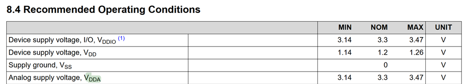
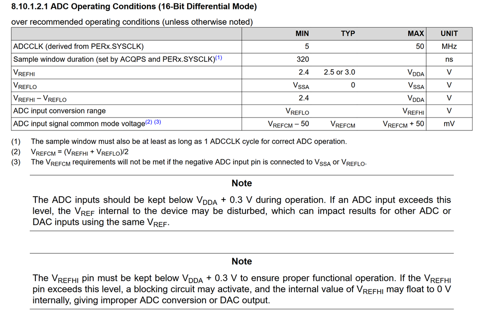
ADC of LaunchXL-F28379D in the latter stage is VREFHI = 3V, so the maximum convertible voltage by the ADC is 3V.

Is this voltage difference a problem in use?

Koki

  • Hello Koki,

    In general, there's no harm from a functional standpoint. It just helps with noise immunity if the ADC ref and CSA ref are tied to the same node.

    To step back and review to the functional overview of the ADC + CSA circuit, the ADC reference voltage determines what the equivalent full scale value is. So if we have 3V on the ADC Reference and I apply 3.1V, the ADC still sees the equivalent of 3V. Moving back to the CSA, it is powered by AVDD, which is around 5V. The CSAs: Current Shunt Amplifiers section in the datasheet shows the equation for SO (or output) which eventually goes to the ADC input. We know that SO can swing higher than 3V (and almost up to 5V or AVDD) if the correct criteria is met in the equation. According to the equation, VREF is independent of the ADC reference voltage so, it doesn't matter what VREF or AVDD is, as long as SO is controlled to be below the reference used at the ADC (3V).

    Best practice dictates that the reference voltage used by the ADC is the same as the reference voltages used by the amplifier stage, so the voltage scaling at the ADC has some dependency on the output of the CSA. If noise couples into both is effectively "the same" then the output of the SOx and ADC full scale value will change by the same amount. This is the benefits to having the ADC and CSA on the same reference rail.

    So, if you don't have this benefit, you'll just need to be conscious that if noise is seen other either rail, that you'll need compensate or calibrate for it.

    Best,

    -Cole

  • Hi,

    Thank you for your kind answer.

    When SO of CSA exceeds 3V (like 3.3V), the ADC recognizes it as a 3V input.

    In this case, is it necessary to set  ADC VREFHI to 3.3V ?

    Or do I need to control SO within 3V?

    Or do I need to do neither? (I think there is a limit to the maximum input voltage of the MCU...)

    Thanks,

    Koki

  • Hello Koki,

    Damaging the ADC:

    Looking at the datasheet, it looks like VDDA is 3.3V typical, with an abs max of 4.6V (in relation to VSSA) where the maximum V_REFHI should be at VDDA or typically around 3V. The notes say the inputs and V_REFHI should be kept below VDDA + 0.3V or risk damage. See applicable tables below. So, 3V or 3.3V for the V_REFHI works.

    This means, exposing at the typical VDDA (or 3.3V) at the input, should be fine for operation but the output of the ADC will treat it as 3V (assuming _VREFHI is 3V). I don't know enough about ADC's as to why the default or typical configuration is that the reference voltage is less than the supply voltage for the ADC, but I'm sure there's a reason because its very very common.

    On the DRV side and SO:

    According to the equation in the DRV datasheet, the output of the CSA is an inverting signal. That means, positive current makes the output lower. Another way to say this, is that at no current, you'll be at VREF/(k_divisionFactor or whatever is mentioned in the datasheet), and the maximum current will be closer to GND.

    Unless you're measuring negative current is well, then there really isn't an issue with trying to keep the SO pin voltage below 3V or the ADC ref. If you do want to measure negative current, then you divide the reference smaller and size the shunt resistor and gain so that the most negative current is around 3V or 3.3V, no current is around VREF/k_division, and maximum positive current is around 0V.

    So, all of the things you presented are possible depending on what kind of performance or current per bits, or current per ADC input volts you want to measure.

    Best,

    -Cole