This thread has been locked.

If you have a related question, please click the "Ask a related question" button in the top right corner. The newly created question will be automatically linked to this question.

DRV8302: DRV8302DCA gate driver IC design problem

Genius 9880 points
Part Number: DRV8302

Hi Team,

Customer encountering problem in their design. Below is the inquiry.

"

My issue is with a circuit based on a DRV8302DCA gate driver IC.

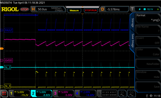
I'm building a BLDC driver, the FAULT signal gets triggered every time I command the L3 MOSFET to turn on. I found on another post the cause could be a GVDD undervoltage, and it is.

The strange issue is it only happening for that particular MOSFET, and it's not the MOSFET's fault, as I have swapped it with L2 and the problem persisted

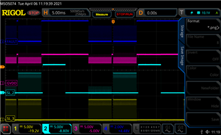
As you can see in the second picture (8) the gate voltage for L3 never rises as much as L2 and in the first the FAULT triggering is correlated with L3.


I have previously fried the chip becouse due to a mistake the SH_x lines were not routed, and when adding them with exterior wires two of them got swapped. After replacing the circuit was first turned on without them, but they were quickly added when both FAULT and OCTW kept triggering, which made them stop, well, at least for this exception.

---------------------------------------------

I have since made more measurements and found out the resistance between pins 36 and 38 to be of 27 ohm, much lower than the observed in the other channels. Thus the problem appears to be another fried chip

"

Regards,

Maynard

  • Hello Maynard,

    Thanks for posting to the MD forum!

    Can you share the schematic of your board? Are your high side FETs operating normally? Can you check to make sure the soldering of the gate driver IC and low-side FETs are sufficient to allow for the LS FETs to turn on and off properly?

    For future reference, when measuring the gate voltages, can you measure with respect from gate-to-source to confirm the gates are not turning on fully for the GL_C?

    Thanks,
    Aaron

  • Hi Aaron,

    Thank you for your kind response. Below is the customer response.

    "The high side mosfets are working normally and the soldering appears to be good. I have since replaced the chip, the circuit started to work. However, after turning EN_GATE low, an then high again the circuit's behaviour became the same, with the new chip measuring 27 ohms across the same pins. In the schematics the SH_x lines were forgotten, but they have since been added via mod wires."

    DRV8302.zip

    Regards,

    Maynard

  • Hi Maynard,

    I'll get to reviewing the customer files and leave feedback by Monday since I'll be OoO today. However, I can state that adding blue-wired SH_x signals will increase the inductance in the bootstrap path, especially if SH_x is blue-wired to both the switch node and the bootstrap capacitor. This may result in voltage brownout on the GVDD regulator when switching at the phase since the added inductance is making the current path for the bootstrap likely to have inductive spiking. 

    Thanks,
    Aaron

  • Hi Maynard,

    I looked over driver and powerstage schematics and have the following feedback:

    - If the main board connects into the ESC inverter board through the large 2x22 header, then you will have a lot of inductance on the gate drive paths. This inductance in combination with added inductance from blue-wiring the SH_x signals to the powerstage can disrupt the bootstrap path and cause current spiking that will brown out the GVDD regulator. It is recommended to make the gate drive paths as short as possible to lower system inductance.

    - I believe the gate drive current settings are non-configurable, so the FETs are likely being turned on to quickly due to large gate drive settings (1.7/2.3A peak). Qgd of FETs = 9nc, so you may be turning on the MOSFETs very quick if the 4.7ohm gate resistor does not limit the current much. Try increasing gate resistance and 

    - nFAULT needs >10k pullup to detect faults since it is an open drain pin

    - 4.4uF of capacitance on DVDD may cause slow voltage rise and large current absorption upon startup

    This thread has lots of pertinent information in regards to DRV8302 layout, debugging, and troubleshooting: https://e2e.ti.com/support/motor-drivers/f/motor-drivers-forum/684448/drv8302-gate-drive-troubleshooting

    Thanks,

    Aaron