This thread has been locked.

If you have a related question, please click the "Ask a related question" button in the top right corner. The newly created question will be automatically linked to this question.

LM5170: VINX has no voltage

Part Number: LM5170
Other Parts Discussed in Thread: , LM6144

Dear TI Team,

I have tested the EVB with LM5170 and now in a more complicated context, I have built this stage as a second stage after the main stage in my prototype.
At the moment I have the difficulty that nFAULT (pin 27) is not above 2.5V and VINX (pin 4) is not switched through and takes the voltage from VIN.
At the moment I don't understand the problem. All input voltages are there. UVLO (pin 10) is coupled to 10V and has about 6V.
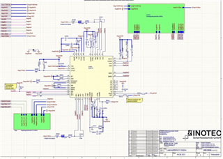
ISETA pin 45 is affected by voltage regulation as follows:
Here in the lower schematic "ChrgVCC" is equal to the above pin "Chrg10VDC" (10V input voltage).

ISETD is accordingly on GND.

Can you please contact your colleague for this product and give me feedback?

Before I made my schematic design I used the calculation Excel "LM5170DESIGN-CALC" made by TI.

  • Hi Robert,

    Thank you for selecting LM5170. The VINX issue could be caused by the nFault low. And the nFault issue could be one of the MOSFETs failed the fault detection. You can check if their drain-to-source are shorted.

    Thanks,

    Yinsong

  • Dear Yinsong,

    All MOSFETs are checked before. But I have seen a big mistake. In the first picture, the R5002 has 24kOhm instead 24Ohm. The VCCA Voltage is dropped to 2.5V. In this case, I recognized that the analogue part does not really run. I changed the value from 24kOhm to 24Ohm and the chip is running. But now I have the next question. the output voltage gets a sawtooth signal form. The reason can be that i didn´t implement the filter at shunt measurement, right?

  • Hi Robert,

    Thank you for the update. For the new question, could you possibly show the waveform? If we are talking about the switching-frequency ripple, that is normal.

    Thanks,

    Yinsong

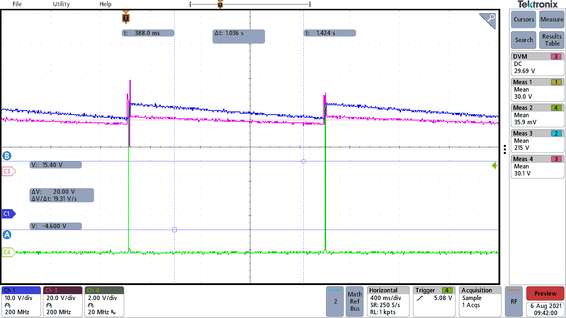
  • Large Signal Output VoltageIf the MOSFETs are On

    Dear Yinsong,

    all pictures are followed defined:

    dark Blue is Output voltage

    red/magenta is Switching Gate on High-side MOSFETs

    green is Switching Gate on Low-side MOSFETs

    For me it looks like non-right switching. I looked for the sawtooth signal on HB pins. The peak value is over 2.6V. Maybe this is too small for the MOSFET Type. The datasheet is attached.

    TPH3R70APL_datasheet_en_20191017.pdf 

    I have checked all regulation parameters for current and outer voltage. The result is, that changing the parameters does not have an effect on this issue. Also, a change of filtering of shunt resistors für CSA and CSB pins does not have an effect.

  • Dear Yingsong,

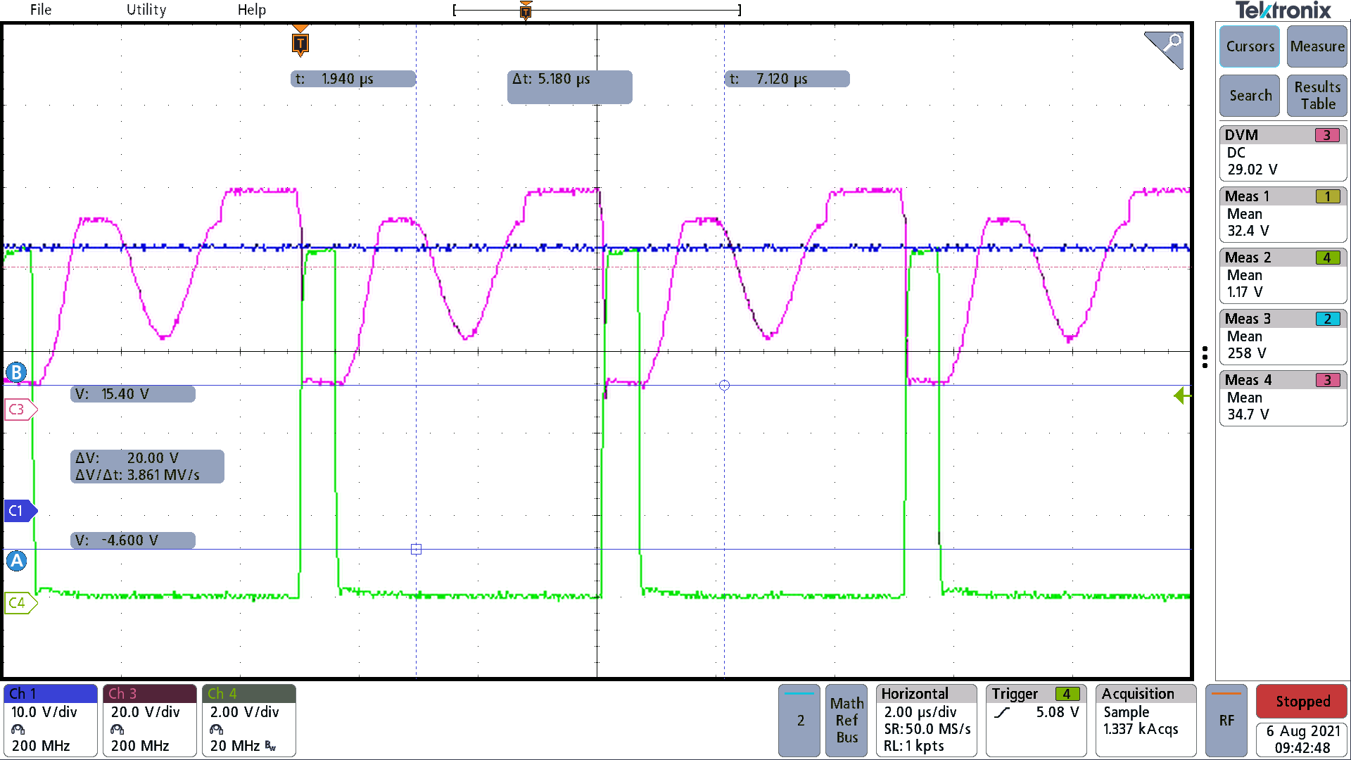
    I have checked the sawtooth signal on Ramp pins.  I have forgotten to explain that these signals are measured under light load.

    In both pictures the dark blue signal is the HB pin to charge the drive signal for the gate on High side mosfet (still red signal).

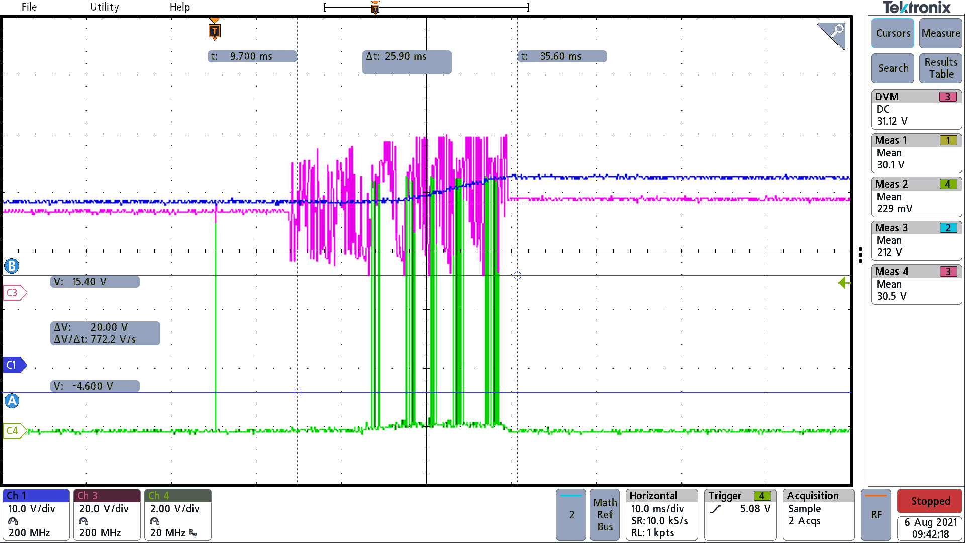
    Large Signal Output VoltageIf the MOSFETs are On

    Dear Yinsong,

    all pictures are followed defined:

    dark Blue is Output voltage

    red/magenta is Switching Gate on High-side MOSFETs

    green is Switching Gate on Low-side MOSFETs

    For me it looks like non-right switching. I looked for the sawtooth signal on HB pins. The peak value is over 2.6V. Maybe this is too small for the MOSFET Type. The datasheet is attached.

    TPH3R70APL_datasheet_en_20191017.pdf 

    I have checked all regulation parameters for current and outer voltage. The result is, that changing the parameters does not have an effect on this issue. Also, a change of filtering of shunt resistors für CSA and CSB pins does not have an effect.

  • Hi Robert,

    Thank you for the waveforms. Could you please confirm the information

    Is it in Buck mode?

    What is the input voltage and target output voltage?

    +one thing that I do not understand is that in the zoom in waveform, the HB dark blue is much smaller than the HO pink. Do you already probe the differential voltage HB-SW for dark blue or I misunderstood?

    Thanks,

    Yinsong

  • Hello Yinsong,

    the converter is in buck mode and the target output voltage should be adjustable between 21V and 29V. The input voltage is 48V. In the showed curves the actual adjustment was to 28V. It seems that the converter starts gets 32V, and stops, like a bang bang controlling between two voltage levels. The OVPB Pin is defined with 37V OVP on buck mode.

    The regulation part as I have described before are tested with original values from EVB and calculated values via Excel-sheet in design files for LM5170-q1.

    In both cases, the output voltage still reacts as described.  

    I have seen similar problems on Ticket "LM5170-Q1: LM5170 boost converter has not stable output voltage, when not loaded".

    So what I additionally have tested is, that changing the capacitance from 10nF to 100nF on SS-Pin does not have an effect on this issue.

    But if you see the measurement below, the SS-Pin is discharged. So what can it be? So the converter is definitely in restart mode.

    red: SS-Pin

    dark blue: output voltage with maximum value 32V

    blue: Drain Source HI-side MOSFET

    green: Gate LO-Side MOSFET

    red: SS-Pin

    dark blue: output voltage with maximum value 32V

    blue: Drain Source HI-side MOSFET

    green: input voltage 48V

    Buck Mode, light load

  • Hi Robert,

    Do you mean that this Vout and SS rise and fall happens continuously?

    If the target output voltage is 28V, it seems it is already good before the SS starts to rise? After SS rises, the output voltage is actually above the target output?

    For the SS pull down, you might want to actually monitor the OVPB voltage to first ensure it's not the OVP issue.

    Thanks,

    Yinsong

  • Dear Yinsong,

    with the curves I wanted to represent that in principle the soft start is started when the output voltage falls below the set reference value. This runs until OVPB is reached. I have checked the OVPB. 1.185V is reached. I am surprised because mathematically I set this to 37V (33kOhm on OVPB pin with 100pF capacitance as suppression). But in the measurement curves this is already the case at 32V. The converter switches off until the voltage falls below 28V and then restarts via softstart. I have no approach at the moment. Because if I reduce the resistance at the OVPB, so that the overvoltage should be higher, I do not prevent this process.
    Actually, the voltage regulation must intervene. Therefore, I currently do not know why this behavior exists.

  • Hi Robert,

    I see. It is strange that a resistor divider does not work..

    Have you measured the 33kohm resistor with a multi-meter?

    And does this happen on multiple ICs or just one?

    Thanks,

    Yinsong

  • Dear Yinsong,

    the resistor has a value of 33kOhm. So that was not the problem. The problem is to have to know, that the lm6144, used in EVB for outer voltage regulation, is an output rail to rail opamp. So if the inverting input is equal to or bigger than the non-inverting input in its value, the output is 0V. The standard opamps do not work like described. A standard opamp has always an internally virtual middle point (Common Mode) as reference. So it means, that if inverting input has the same or bigger value as non-inverting input, the output of the opamp has the middle value off VCC-VEE. If you use this opamp between 0-5V, the output has then 2.5V at the difference between the input is 0.

    In this case, if the inverting input has a bigger voltage than the non-inverting the output voltage is <2.5V but bigger than 0V!

    So the ISETA has a set value > 0V and that means for current regulation to pump energy in the system regulated to the set value. This caused the overvoltage on output and the overvoltage output setting as described in the datasheet will be activated.

    So what I finally want to say is, that in the datasheet and in EVB-manual the importance of the rail to rail output opamp is not described. But this is necessary! Additionally, my problem is solved now. 

  • Hi Robert,

    Thank you for the information and sorry for the confusion.

    Thanks,

    Yinsong