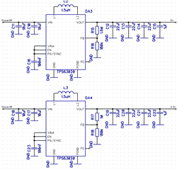
Other Parts Discussed in Thread: PMP9769
Hello, I am designing a device using two TPS63020 converters (somewhat similar to PMP9769) and have a couple of questions:
1) In the PMP9769, the VIN and VINA inputs of TPS63020 are connected, though the reference schematic and layout in the datasheet does not show any connections between these pins. What is the right schematic?
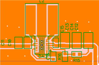
2) Currently I have 2 converters on a single board (one working mostly in boost mode, 4.2V->5V, and one in buck mode, 4.2V->3.3V), and both exhibit the same strange behaviour while the output current is low - the input current (even in "quiscient mode", when the loads are disconnected) does not drop below 10 mA, which is much larger than the 25-50 uA indicated in the datasheet. What possibly could be wrong in the schematic and on the board (the layout for both of the converters is similar, so only one is attached):