This thread has been locked.

If you have a related question, please click the "Ask a related question" button in the top right corner. The newly created question will be automatically linked to this question.

UCC27211: G-S signals missing occasionally

Part Number: UCC27211

Dear All,

I am using UC27211 for a three-phase motor driver. A UC27211 drives six  MOSFET (Part No.: IRF7769L1), three on the upper arm in parallel and three on the lower arm in parallel. The schematic of one phase is shown in Figure 1 below. The bootstrap capacitor is 4.7uF. The turn-on gate resistor is 2Ω. Turn-off gate resistor is ideally 0Ω, by using a reverse diode.

Figure 2 shows the output voltage. Please ignore the negative polarity of the waveform caused by the measurement. The pulse width of the PWM signal is about 1.5us.  The normal waveform is good, with fast turn-on and turn off transistion.

However, there is abnormal waveform occasionally observed. It seems that the mosfet is turned-on firstly, then back to off immediately, and then tries to turn-on again. Please note that low voltage means on state.

It can be also observed that the G-S signal is missing occasionally, which causes the abnormal output voltage.

This phenomenon happens when the DC-link voltage increases to 30V. At 20V DC-link, no abnormal waveforms are observed.

Could anyone provide a solution to address this issue? Should I increase the turn-on resistor?

Thanks!

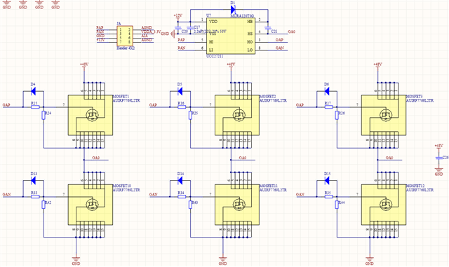
Figure 1: Schematic of the gate driver for six mosfets.

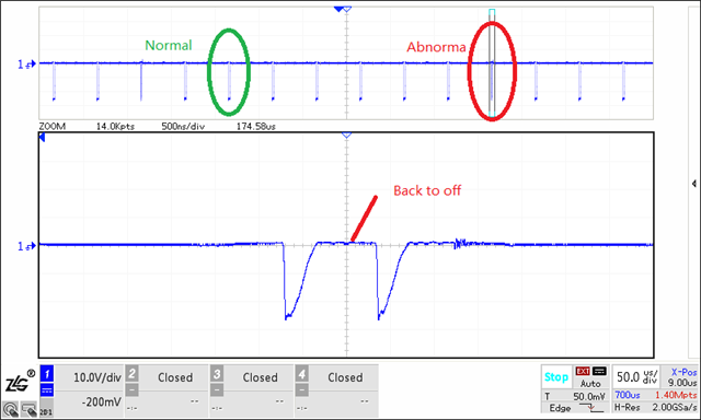
Figure 2: Phase Output Voltage (Please ignore the negative polarity of the waveform caused by the measurement).

Infineon-IRF7769L1-DS-v02_00-EN.pdf

  • Hello Jiaxiang,

    Thank you for the interest in the UCC27211 drivers. We will be able to help with your concerns but I need to ask and confirm some information to better assist.

    You mention the boot capacitor is 4.7uF which is fairly large value, so we need to confirm the HB-HS bias is being fully charged and the bias is maintained during switching. We usually recommend the VDD capacitance be 10x the boot capacitance value to minimize excessi8ve VDD voltage drop when charging the boot capacitor,. I see 2.2uF for one VDD cap but no value on the other, can you confirm there is adequate VDD capacitance relative to the 4.7uF boot capacitance?

    Also one consideration of the HB bias with low frequency switching, is that resistance on the gate to source will discharge the HB capacitor. Can you confirm the value of the gate to source resistance? 

    Besides the bias concerns, it is possible there may be unexpected voltage spikes or ringing on the driver inputs which could cause unexpected driver output behavior.

    Can you monitor the gate driver LI and HI inputs along with the unexpected output behavior to confirm there is not excessive voltage spikes or noise on the inputs?

    Also for scope measurements, monitor the HB-voltage with a scope probe to confirm the bias is above UVLO during the unexpected output behavior.

    Confirm if this addresses your questions or you can post additional questions on this thread.

    Regards, 

  • Hi Richard,

    Thanks for your reply. The boot capacitor is selected 4.7uF based on trial-and-error. The input capacitance of each mosfet is 11.56nF. The total input capacitance of three parallel mosfets is then 34.68nF. Initially, 470nF is selected. However, the boot voltage drops to lower than 8V during the turn-on period. Therefore, I then increased the boot capacitor to 1uF and finally to 4.7uF. We haven checked the boot voltage waveform. The boot voltage is good when the unexpected output behavior occurs.

    The G-S resistor is 4.7kΩ. I thinks this is large enough. 

    I will try the options you suggested. Thanks.

  • Hello Jiaxing,

    If there is long HO on times the gate to source resistance is a consideration to change (increase) if you do find that the HB-HS voltage is dropping during the operation. Depending on if HB-HS discharge is a concern, it may be advised to increase the gate to source resistance.

    Keep me posted on the findings based on my suggestions. We may have to do more investigating of the operation depending on the results.

    Regards,

  • Dear Richard,

    Thanks very much for your suggestions. I have solved this problem as follows:

    1) I measured the D-S waveform and the VDD voltage simutaneously. It was clear that there was dips on the VDD waveform. I suspect the dips caused the UVLO protection of the IC and shutdown all the mosfets. Therefore, I increase the capacitor at the VDD pin to 10uF. The dips disappeared and the converter works fine now.

    2) I also suspect that the turn-on speed is too fast, which may be the cause for the dips on VDD waveform. Therefore, I also increase the gate resistors of all the mosfets to 12Ω.  I am not sure if this is the key factor that addresses the issue, but I think higher gate resistor should be better.

  • Hello Jiaxing,

    Thank you for confirming the resolution to your issues, and describing the findings and fix. This is helpful to others on the forum.

    Regards,