This thread has been locked.

If you have a related question, please click the "Ask a related question" button in the top right corner. The newly created question will be automatically linked to this question.

LM5116: Occasional failures, cause unknown

Part Number: LM5116
Other Parts Discussed in Thread: CSD19531Q5A

Hi there,

We have a board designed for 5.2V 6A and 7.4V 18A output running of 30-48V. We are seeing some failures during operating as well as at power on. There are also boards which work fine and temperatures do not exceed expected values. 

In one case the LM5116 chip burnt out and in the other the voltage is lower than expected and the other chip is heating up. Some of the boards are working just fine. Both the 7.4V layouts and 5.2V layouts are very similar and based on the guidelines in the EVAL board: www.ti.com/.../snva285a.pdf    

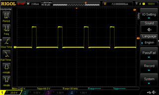
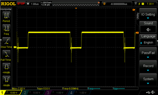
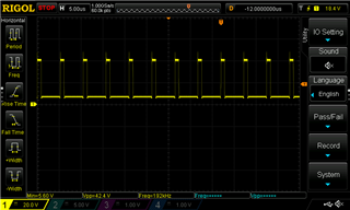
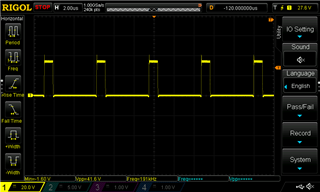
What I am seeing when measuring the HO and LO on the mosfets the LO has a very negative spike at high currents and I am wondering if this is the cause of the failures? It seems that some negative transient here is inevitable according to the posts I have been reading. Is there anyway to verify that this is what has been causing the LM5116 failures e.g by measuring the failed chips in some way?

I also noticed our CSD19531Q5A mosfet 226nC QRR is relatively high, could this be causing the negative spikes? 


HO, LO, SW (pin 20), HB (pin 18)

I think the component selection and layout should be okay as per the excel design, I have attached them as well for reference.


0284.PCB.pdf8345.Schematic.pdf

  • Hi Steven,

    Looks like there's a lot of Cdv/dt coupling to LO from the rising SW voltage. This ringing may cause a slight amount of shoot-through if the low-side FET turns on for a short time.High Qrr doesn't help as it may increase the ringing on SW and thus the coupling to LO (although your SW waveform looks relatively clean - check that you're measuring right at the FET without probe bandwidth limit)

    One option to reduce that is slow the high-side FET turn-on with a gate resistor or a resistor in series withe the boot cap. Also, given Vin-max = 48V, maybe you can try 60V FETs for better efficiency / cleaner waveforms (especially for the high-current design). Note that it is imperative to have the input caps close to the FETs - see app note snva803 for more detail.

    You may want to check what pins of the IC are getting damaged (for example, LO or HO). Also, send along the layout for review.

    Regards,

    Tim

  • Thanks a lot for the info Tim, that makes a lot of sense. Do you think that having an RC snubber on the SW output would be necessary/make a difference? I am also thinking of adding schottky diodes to protect the gate driver pins from negative voltages. It would be great if you were able to have a quick look at our layout, the Schematic and PCB overview are attached to the previous post as PDFs.

    Regards,

    Steve 

  • Hi Steve,

    The key is to key the gate loop areas as small as possible, thus minimizing gate loop inductance. For example, route HO and SW as parallel traces with traces widths greater than 20 mils. Your layout looks good with the input caps close to the FETs. Just ensure that a closely spaced GND plane (6 mils intralayer spacing) is used on layer 2 right below the power stage.

    Regards,

    Tim