This thread has been locked.

If you have a related question, please click the "Ask a related question" button in the top right corner. The newly created question will be automatically linked to this question.

TPS7A24: PCB layout for measurement of Rθja

Part Number: TPS7A24

Hello team,

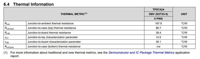
What is the PCB layout for measurement of Rθja?

I read "Semiconductor and IC Package Thermal Metrics", but I could not find it.

My customer wants to know "number of layers" to consider their layout before they receive samples.

Best regards,

Shotaro

  • Hello Shotaro,

    I believe this app note will be helpful to your customer.

    https://www.ti.com/lit/an/slvae85/slvae85.pdf

    The thermal resistance and parameters in the datasheet are based on the JEDEC standard, High K approximation.  The High K approximation is the most popular metric used by designers to evaluate board performance.  Our EVM's are closer to the JEDEC standard, thermally saturated approximation.  So when you test our EVM's, you will see a significant thermal improvement over the published junction-to-ambient thermal resistance listed in the datasheet.

    Once you have the fabricated hardware ready for testing, you can determine your junction-to-ambient thermal resistance by following the steps in this app note:

    https://www.ti.com/lit/an/slva422/slva422.pdf

    Thanks,

    - Stephen