This thread has been locked.

If you have a related question, please click the "Ask a related question" button in the top right corner. The newly created question will be automatically linked to this question.

TPS40305: Getting the EMI peaks

Part Number: TPS40305

Hello Peter,

We have incorporated below list of changes in the design.

FB15= 330ohm ferrite bead (MPZ2012S331AT000)

C589= 820pF

C590= 22uF

C101=10nF

R789= 3R3

R790=10R

also added 0.1uF on parallel to C590 & C64

I have added 3R3 resistor between boot pin and C85(0.1uF)

Snubber value is the 5.1R and 150pF.

Here is the Switching & EMI result on in-house spectrum analyzer.

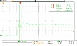
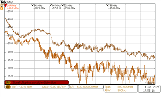
still we are getting the major ~200MHz peak.

Let us know how to remove this 200MHz peak. 

Also other noise are improved respect to previous results but still its not good to go for final certification.

also i have changed the snubber value 2R2 & 2.2nF

Here is the results.

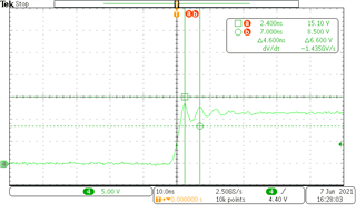
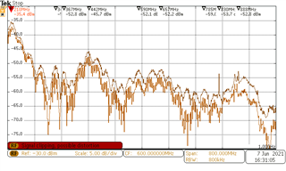
Let us know the snubber value range to test various combination.

  •  

    The best procedure for optimizing a snubber is:

    1) Remove the snubber and measure the resonant oscillation frequency

    2) With a 0-ohm resistor, add snubber capacitance until the resonant oscillation frequency is cut in half

    At this point the total capacitance is 4x larger than with no snubber, so the internal parasitic capacitance is 1/3 the added snubber capacitance

    3) Calculate the internal parasitic switch-node capacitance (1/3 snubber capacitance) and the parasitic inductance

    Lpara = 1 / (4 x π^2 x Fres x Cpara)  (If you use the frequency without the snubber, it's just Cpara, if you use the frequency with the snubber, it's Cpara + Csnub

    4) Calculate the characteristic impedance of the L-C resonance (include the final snubber capacitor you will use.

    Zcharacteristic = Sqrt [ Lpara/ ( Cpara + Csnub ) ]

    Selecting that resistance for the snubber resistor will provide the optimum reduction.

    While increasing Csnub will reduce the ringing amplitude, the amplitude reduces as the square-root of the capacitance.  Beyond Csnub = 3x Cpara, the benefits of further increases in snubber are small.

    Another place to look for 200MHz noise reduction would be to improve the bypassing impedance from Drain of the high-side FET to the source of the low-side FET to supply current to charge up the switching node in a tighter, lower inductance loop.  In my experience, a small, 0402 capacitor of 2.2-10nF as close to the drain and source as possible helps a lot.  In addition, staggering output capacitors in 1/3 steps (10uF, 3.3uF, 1.0uF, 0.33uF, 0.1uF) with capacitors on top and bottom of the PCB, and VOUT between ground connections helps minimize the output impedance at very high frequencies to minimize conductive noise.

    Also, I don't see your schematic for the reference of the locations you're naming, so I don't have a point of reference for those changes.  It does not look like adding 2.2nF of snubber capacitance shifted the resonance frequency much, which suggests that there is a lot of parasitic capacitance on the switching node.