This thread has been locked.

If you have a related question, please click the "Ask a related question" button in the top right corner. The newly created question will be automatically linked to this question.

TPS62861: power good signal

Part Number: TPS62861
Other Parts Discussed in Thread: TPS61240

Hi team,

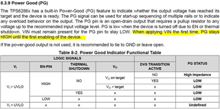
My customer would like to use the TPS628601 power good signal drive the enable of the TPS61240 to sequence the two power rails.  Section 8.3.9 in the DS says that the signal can be used for just that purpose. However further down in that section it states that it  doesn’t actually work until the device is enabled (see yellow highlight below). The design requires an I/O signal to control the power enable (i.e. we can just tie the enable to Vin).

So is section 8.3.9 accurate?  If so, is there any recommended work around?  The design is a very tiny module, and there's no room for adding other ICs such as an external power sequencer. 
 

Regards,

Connie


  • Hello Connie,

    I will test the EVM to check if there is a possible workaround to overcome your concern with the PG pin signal. Give you an update tomorrow.

    Best regards,

    Excel

  • Hello Connie,

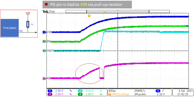
    The PG pin goes High during the turn-on delay phase (Vout < 96% of Vout). And if the pull-up resistor is tied up to VIN or external supply, it will prevent your application from having the proper sequencing. See sample waveform below.

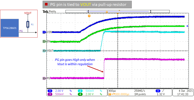
    A possible workaround is to tie the PG pin to Vout via a pull-up resistor. This way PG pin will only go High when the Vout is within the target level (PG is always Low during the turn-on delay phase). And proper sequencing will be achieved.

    However, the limitation of this solution is the PG voltage level is dependent on the Vout level. If the Vout is lower than the EN pin High threshold of the other circuit, then this solution will not work. 

    Is the above solution works in your application?

    Best regards,

    Excel

  • Hi Excel,

    Thanks for the info.  Unfortunately, my customer's design uses the TPS628601 to create 0.8V which is below the Vih_min (1V) for the enable on the TPS61240.  So this workaround won’t work for them.

    What about pulling up the powergood signal to the enable signal driving the enable input to TPS628601?  They use a 1.8V signal from an MCU to drive the enable signal. They will need to confirm that signal is actively driven and not open-drain. 

    One other comment regarding the waveforms you show below.  In their application Vin comes up first, then other power supplies turn and an MCU boots.  Then the MCU asserts the enable.  So there will be a considerable delay from Vin going high to enable going high (likely 100s of milliseconds).  I don’t think this helps or hurts.  But I thought I should share this while you are considering other workarounds.

    Thank you!

    Connie

  • Hi Connie,

    I understand. Connecting the PG pin cannot be tied up from the output voltage (0.8V) because it is lower than the EN High threshold of TPS61240, which will not ensure it is triggered properly.


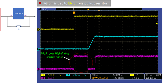
    We tried to tie the PG pin to the EN pin. And as expected, the PG pin will still go High during the start-up delay phase (see figure below) even though the VIN is supplied beforehand. Therefore, it might not solve the sequencing issue. See waveform below details.

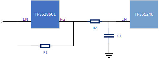
    How about adding an RC network to work as a blanking circuit? Do you think this is acceptable to the customer?

    Best regards,

    Excel

  • Hi Excel,

    Thanks for the support. Customer was able to solve the issue through using another digital signal to sequence the start up of the design.

    Regards,

    Connie

  • Hi Connie,

    Thanks for the update.

    If you need further support, feel free to post your queries here again. In the meantime, I will close this thread.

    Best regards,

    Excel