


Other Parts Discussed in Thread: TPS3422, TPS3420
Hello,
My customer is evaluating the TPS3421 device on the EVM and they are seeing that if voltage is present on either PB pin when VCC is not present, the VCC rails powers up to a diode drop below the voltage on the PBx pin. This seems to mean that there is a diode from PBx input to VCC and that there is no blocking on these inputs.
My question is do either of the other devices in the family behave differently where there is not a diode path from PBx to VCC? My customer would like the ability to have a voltage present on the PBx pin without the device powering up.
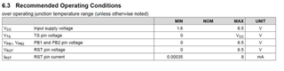
Looking at the datasheet the TPS3420 has "NMOS based threshold" whereas the TPS3421 has standard CMOS input thresholds (0.7*VCC) and the TPS3422 doesn't need a pull-up and the TPS3421 does externally. Basically there are differences but I cannot tell if this is one of them. Also, looking at the recommended operating conditions it isn't clear that PBx voltage and VCC are related. If the PBx voltage was listed as VCC + 0.3V it would be clear that there was a diode path (instead of independent 6.5V regardless of VCC).
Let me know and thanks!
John

