This thread has been locked.

If you have a related question, please click the "Ask a related question" button in the top right corner. The newly created question will be automatically linked to this question.

TL431: Design Guide: TIDA-01605

Part Number: TL431
Other Parts Discussed in Thread: TIDA-01605

Hi TI team,

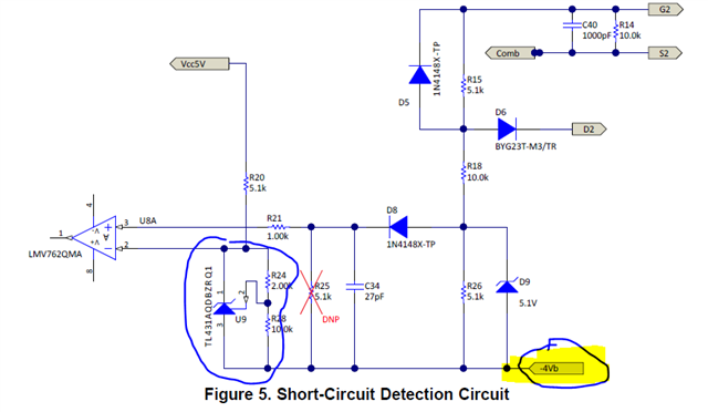
The picture below was taken from TIDA-01605 reference design. The TL431 in blue circle is used to create 3V reference for the comparator.

However, the anode of TL431 is connected to -4V potential. Since the output voltage is 3V, the potential of Cathode is -4V + 3V = -1V.

I tried to simulate this circuit in LTspice as shown in the right picture. However, I noticed that whenever I connected TL431's anode to -4V, it did not work. TL431 only works when its anode connected to 0V.

Could you explain this issue? How can the TL431 work when it's anode is connected to -4V as shown in the schematic of reference design?

In reality, does it matter if we connect its anode to a negative or positive voltage for reference?

Thanks a lot!


  • Hi Van,

    The spice model is written such that it only operates at "normal" typical conditions like GND = 0V. 

    The concept of GND is associated with 0V where it is the lowest potential.  GND can be any voltage so long as the differential power supply volte is high enough to turn on the device.   Therefore, the "GND" for figure 5 is -4V.  It is considered to be the "ground floor". 

    To answer your question, no, it doesnt matter if you connect  its anode to a neg or pos voltage rails.

    Ben

  • Hi Ben,

    Thank you so much for your response. I understood why my TL431 does not work with negative voltage in LTspice. I have two more questions:

    1) How did you simulate the circuit in Figure 5 in TIDA 01605 with SPICE software? Did you elevate all voltages with the same amount of 4V for all node potentials?

    2) I have a circuit shown in Fig. 1 below. It is about isolated bias supply for gate driver circuit. The isolated ground "GND2" is connected to Anode of TL431 and the Source of Mosfet. Every time the diode conduct, the GND2 will see a negative potential of -1.5V, which is the forward voltage drop of the diode. And this make TL431 malfunction. What is your solution in this case?

    My workaround is that I add a voltage of +3V to the anode of the Diode as shown in Fig. 2 below. So now, when the diode conduct, the potential of "GND2" is 3V - Vf = 3V - 1.5V = 1.5V (a positive value). And with this modification, the TL431 regulate output voltage of my power supply well.

    Do you think this is a good way to solve this problem? What is your method for SPICE simulation if TL431's anode need to connected to a negative potential while GND potential (0V) is elsewhere?

    Thank you so much.

  • Hi Van,

    Since the model is unencrypted, you can edit the model to your preferred preference.

    Your method is what I would have done as well to make the circuit work because the schematic shows you have GND and -4V.  You would need to set the circuit such that "GND" is not 0V but -4V.

    Ben 

  • Hi Ben,

    Thank you a bunch for your response. Below is the Unencrypted model of TL431. There are several 0VDC, which one I should change to -4V?

    Also, is there any document that I can know the schematic used to made this model? I see there are many capacitors and resistors here.

    Thank you so much. Regards,

    .SUBCKT TL431 7 6 11
    * K A FDBK
    R_R18 0 N16955548 1 TC=0,0
    C_C17 N16955362 0 1n
    C_C18 2 6 0.5u
    D_D11 N16976181 N16975344 DCLAMP
    C_C19 3 4 0.08u
    E_E23 2 N16955404 VALUE { {I(V_V16)*15.6} }
    C_C22 N16955548 0 1n
    R_R13 N16955401 N16955404 1 TC=0,0
    E_E27 VREF 0 VALUE { IF(V(11,0)<2.495,V(11,0),2.495) }
    V_V16 N16955401 6 0Vdc
    R_R14 0 N16955362 1 TC=0,0
    X_H8 7 N169559021 IKA 6 TL431_H8
    E_E24 4 N16955473 VALUE { {I(V_V17)*10} }
    E_E28 N16955936 0 11 6 1
    V_V7 N16976181 6 2
    G_ABM2I2 6 N16975344 VALUE { IF((V(3)-V(6))< 0 , 1.73*(V(3)-V(6)) -1U ,
    + -1U) }
    R_R15 N16955470 N16955473 1 TC=0,0
    V_V17 N16955470 6 0Vdc
    G_G4 6 2 VREF N16955936 0.11
    R_R16 0 N16955493 1 TC=0,0
    D_D12 N169559021 N16975344 DCLAMP
    R_R17 N16955529 N16955532 1 TC=0,0
    C_C21 N16955493 0 1n
    E_E25 3 N16955532 VALUE { {I(V_V18)*100} }
    V_V18 N16955529 2 0Vdc
    V_V19 N16985445 0 0Vdc
    .ENDS
    *$
    .subckt TL431_H8 1 2 3 4
    H_H8 3 4 VH_H8 1
    VH_H8 1 2 0V
    .ends TL431_H8
    *$
    .model DCLAMP d
    + is=1.35e-011
    + rs=0.005
    + n=0.001
    + cjo=4.5e-011
    + vj=0.75
    + m=0.302
    + tt=5.04e-008
    + bv=100
    + ibv=0.001
    *$

  • Hi Van,

    Try starting with the ones with 0V DC.  I am not familiar with this pspice code since I was not the one who developed the model nor do I have the schematic.

    Ben