This thread has been locked.

If you have a related question, please click the "Ask a related question" button in the top right corner. The newly created question will be automatically linked to this question.

LM34936-Q1: Circuit can not operate with full load at boost mode or Buck-boost mode ; Schematic review.

Part Number: LM34936-Q1
Other Parts Discussed in Thread: LM5176

In my application , I use LM34936-Q1 for the design:

Vin : 9~14V , Vout: 12V ; max Iout = 15A

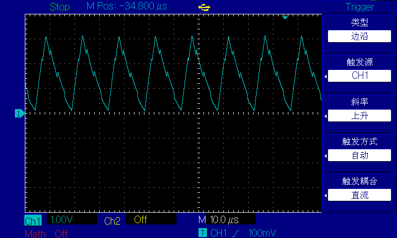
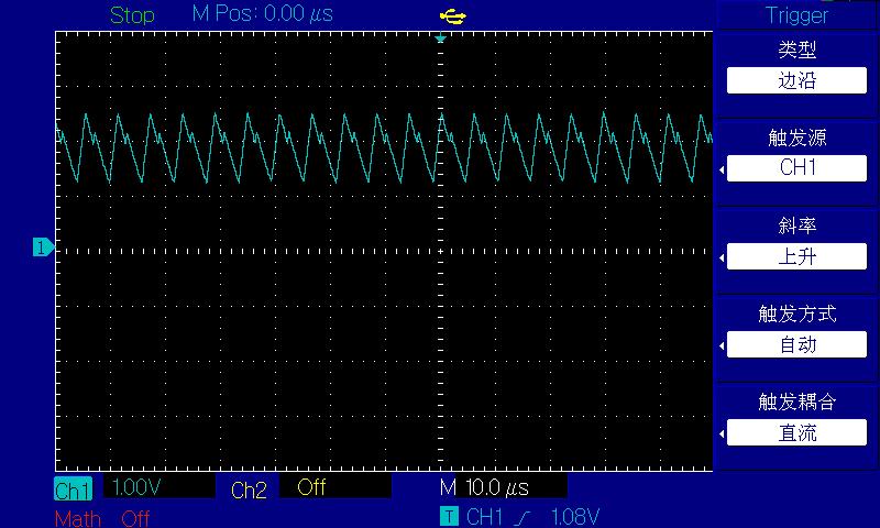
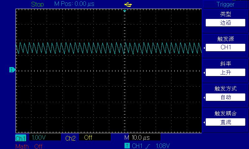
I have already made PCB design and the borad is under debug. In debug process , i found one problem, 

when input voltage is 14.5V , the circuit can drive 15A load normally. (buck mode)

if the input voltage is 9 - 13V, the circuit ONLY can raise load to about 4A.

it seems like that the converter operates abnormally with heavy load when it is in boost or buck-boost region.

this is my Schematic diagram , I would like a kind engineer help me review it and find the design fault.

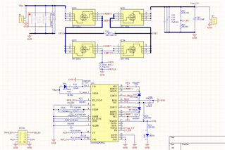
I would also like to listen to more advises for improvement.

for the problem above , i have 2 questions:

  1. Why does this issue happen?

  2. How to solve it?

  • Hello Xinhao,

    Thank you for using our device. When checking the design, some questions came to my mind:

    - Are you using 8 mohm sense resistance or 4 mohm sense resistance. I expect 4 mohm (2 times 8 mohm), but am not sure

    - What is the saturation current of your inductor?

    - How many input capacitors have you populated? There is a box around the input caps which I do not understand. If only the ones outside the box are populated, please test with more input capacitance.

    Can you please send some measurements of the output voltage, inductor current, sense voltage and COMP voltage when the issue can be observed?

    Best regards,
    Brigitte

  • thank you for your reply and considerations.

    I use two 8mΩ/2512 paralleled resistances , i expect 4mΩ according to the design procedure on datasheet.

    for inductor i use SRP1270-1R0M 1uH/2.1mΩ, its saturation current is 50A .

    this module is one part of a device.

    besides two caremic 22uF/0805 capcitor,  about 1mF eletrolytic capacitor has been placed  at the input port , but these eletrolytic capacitors are placed several inches from this module.

    So Do I need more capacitors closed to the module?

    I don't have current probe this time, but I can try to get some waveforms of sense voltage and COMP voltage. there is another problem that, when I use Oscilloscope probe to measure the COMP voltage , the circuit sometimes can not operate normally.

    could you continue checking the design first , I'd also like to get some debug directions. then I can do adjustment within my experiment.

    if you have any doubt , please remind me soon, thanks.

  • Hello Xinhao,

    If there is more capacitance not too far from the converter, it should be ok.

    Please check the VIN voltage as well, that it does not drop to much.

    The schematic seems to be ok, so I cannot tell you really where to start without having a look on the signals.

    In general debugging starts by checking the input and output voltages, the switch nodes, the gate signals, the current sense signal and the COMP signal.

    Especially at startup of the converter, these signals are important.

    Another possibility is to check what happens when loading the module in buck mode and then slowly reducing VIN. When does the output start to drop? How does then the CS vs CSG signal look like?

    Can you please check the capacitive loading of your oscilloscope probe? If you add this to the comp pin it is parallel to the high frequency cap there.

    Best regards,
    Brigitte 

  • Hello Xinhao,

    As I did not hear from you, I expect that you have been able to solve this issue. If this is not the case, please post below or start a new thread if this one is already locked.

    Best regards,
    Brigitte

  • I feel sorry for the long waiting. during these days, we optimize the layout and also purchase a current probe to help us analysis. so we get some waveforms, we do change some parameters due to the waveforms.

    with the current probe, we get the important waveform of the inductor. showing as following.

    All the waveform is for the inductor current. div: 1A/100mV

    I do experiment on this status: Vin = 9V , Vout = 12V

    Problems happen with two conditions:1. heavy load 2. Boost Mode

    Some of abnormal waveform is shown as below, I can't resolve that what is happening.

    the second waveform is operating at 12V12A output. It seems that closed-loop control oscillation exists. Because of the oscillation , the circuit can't operate up to 15A (which is my expection).

    If I reduce the load to about 8A. The inductor current waveform is shown as below

    due to the waveform cycle by cycle , the control loop looks not stable enough, but it operates normally at least.

    Until Now , I use parameter as following:

    Cslope = 100pF (C215)

    Rc1 = 2.7kΩ (R206)

    Cc1 = 12nF (C212)

    Cc2 = Remove (C213)

    I have two questions:

    1. How does the oscillation happen. I wonder the reason.

    2. Would you Help me optimize the control loop parameter. Directions for adjustment would also be welcome.

  • Hello Xinhao,

    Please check out your parameters with this quick design calculator from LM5176. https://www.ti.com/lit/zip/snvc208

    These 2 devices are very similar and therefore the calculator should be able to give you a hint in which direction you need to go with the compensation. In general increasing CC1 makes the system more stable as it reduces the crossover frequency.

    Best regards,
    Brigitte

  • I found the problem has a little relationship with the current sense filter network.

    I used two 100Ω and 47pF to construct the network which the parameters are recommended by the datasheet.

    I tried to reduce the resistor, then the waveform looks better, but problems are not resolved.

    Is there any suggestion about the filter network according to my operating scenario? (Vin = 9~14V Vout = 12V15A fsw = 340kHz)

  • I can make the circuit stable at boost mode now.

    But there is a new issue.

    the strict operation region seems to be the (Vin ≈ Vout )

    With heavy load , when the input is 12V , the waveform of inductor current is like this

    according to the datasheet, I have reduce the Cslope (120pF->68pF) to improve the noise immunity in the transition region, but it doesn't work.

    Is this issue always happened to this IC? Is there any common solution?

  • Hello Xinhao,

    You should not reduce the filter resistors too much as then destortion of the sense signal might occur. Is the filter placed very close to the IC and are the lines to the sense resistor layed out differentially?

    The problems you are observing seem to be noise injection into the regulation. Please try to increase the filter capacitor on the sense lines to 100pF and keep the resistors as you have them now (which value?).

    In addition, you can reduce the SLOPE capacitor to even lower values, but this reduces as well the current capability of the converter at high duty cycles, so you need to check if the current capability.

    Another idea would be to check if you can increase the sense resistor somewhat to increase the noise immunity of the sense signal.

    Best regards,
    Brigitte

  • I try to use 100pF in filter, but problem can not be resolved.

    for the filter resistors, I use two "100Ω" resistors which is recommended by the datasheet.

    For the slope capacitor, I have already reduced to 68pF, which the datasheet calculation recommends 120pF. Can I reduce it even lower?

    Could you help me review the layout of the Kelvin Connection(the current sense signal lines) ?

  • Hello Liu,

    You can reduce the SLOPE capacitor to low values. The difference is an additional slope added to the current measurement which makes it less noise sensitive. So this can make the result somewhat better, but then the maximum output current is reduced and you need to check if it still is able to deliver full current at lowest input voltage.

    Yes, I can review your layout. Did you place the filter components close to the IC?

    Please find here some technical articles on 4-switch buck-boost converter layout:

    https://e2e.ti.com/blogs_/b/powerhouse/posts/four-switch-buck-boost-layout-tip-no-1-identifying-the-critical-parts-for-layout

    https://e2e.ti.com/blogs_/b/powerhouse/posts/four-switch-buck-boost-layout-tip-no-2-optimizing-hot-loops-in-the-power-stage

    https://e2e.ti.com/blogs_/b/powerhouse/posts/four-switch-buck-boost-layout-tip-no-3-separating-differential-sense-lines-from-power-planes

    https://e2e.ti.com/blogs_/b/powerhouse/posts/four-switch-buck-boost-layout-tip-no-4-routing-gate-drive-and-return-paths

    Best regards,
    Brigitte

  • BuckBoost.PcbDocBuckBoost_12V.SchDoc

    This is the PCB file and the schematic Diagram, and I have removed all the unrelated components in PCB diagram.

    If these 2 files cannot be opened, please remind me.

    Thank you for your kind supportion ,helping me review them.

    Best wishes.

  • Hello Xinhao,

    As far as I understand, the converter delivers now in all regions the full load and regulates the output voltage properly. Is this understanding correct.

    When I reviewed the schematic and layout, both seem to be ok, even if I do not like 90 degree angles in a layout. Only the bulk input capacitors seem to be a bit far away from the power stage. You might check if moving one of the bulk capacitors closer to the ceramic input capacitors help to reduce noise on the input side.

    Can you please measure as well the current sense signal CS to CSG? In addition it would be intersting to have a look on the feedback and COMP signals to check if these can somewhat explain the inductor current.

    Please check as well with a SLOPE capacitor of 47pF.

    Best regards,
    Brigitte