This thread has been locked.

If you have a related question, please click the "Ask a related question" button in the top right corner. The newly created question will be automatically linked to this question.

LM3481: Output Voltage when Input Voltage is Increased Gradually

Part Number: LM3481

Hello,

I have a question of LM3481 SEPIC circuit in our design. Input voltage of our system ranges from 4.75V to 24.5V, output voltage of SEPIC circuit is 5V (VCC in the schematics below) with up to 1.2A capacity. This VCC is converted to 3.3V with another regulator, then that 3.3V is converted to 1.5V with another regulator again.

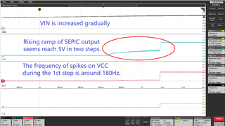
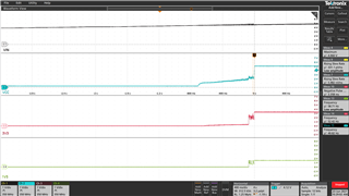
When input voltage is turned on directly, all the power rails seems fine, the system can work normally. But when the input voltage increased gradually from 0V to 5V, it is found that it takes VCC about 1 second to slowly climb to around 2V and then go up to 5V. When VCC is around 2V, there is fluctuation on 3.3V and 1.5V, which potentially breaks the sequence requirement of 3.3V and 1.5V. As a result, the system can't work normally.

We tested LM3481 SEPIC EVM board, connect its VOUT to VCC in our system. When we increased the input voltage from 0V to 5V gradually, we found its output rising ramp was quite stable and there was no problem on 3.3V and 1.5V either.

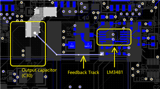
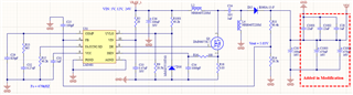
I checked all the components with LM3481 datasheet and AN-1484. It seems there is no obvious problem except that the output capacitor doesn't have enough rated ripple current and low enough ESR (There are some capacitors for VCC at other locations of the board), so I added some more capacitors at the output as shown in the schematics below. It could only reduce some noise (fluctuation) on VCC but still could not make a beautiful (linear) rising ramp.

I am wondering if you could suggest if there is anything wrong in my design. Thank you!

Here is the schematics

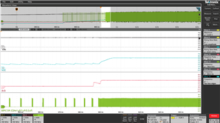
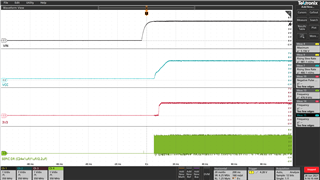
Below is the measurement of input voltage (VIN), VCC, 3V3 and 1V5 when VIN is increased gradually.

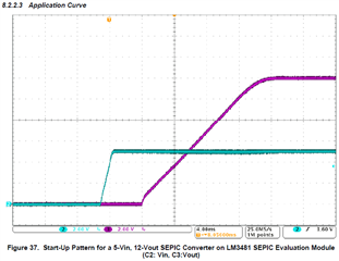
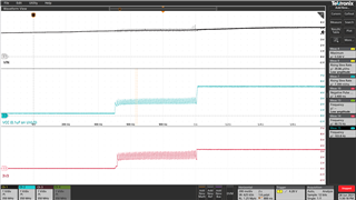
Below is a start-up waveform from LM3481 datasheet. We found when LM3481 SEPIC EVM is connected with our system, VCC has a very clean rising ramp (similar to the picture below).

  • Hello, 

    Thanks for reaching out. The first thing that I would like to suggest is the following: I see that the first output cap on your schematic is a polar one (likely an electrolytic one). I would suggest to place the electrolytic one as last one and place the ceramic caps with low ESR closer to the converter. It always helpful to have ceramic caps with low ESR close to the power stage also because the ESR of the cap is introducing and additional zero in the Bode plot and this might sometimes cause troubles.  In you layout, is the FB divider connected like it the schematic or is it connected after the output caps? 
    Let me know if I can help you furthermore. 

    Kind regards, 

    EM

  • Hi EM,

    Thanks for your reply. I tried to add a ceramic capacitor beside C30, which is very close to the output of SEPIC circuit. The problem is still there. The graph below shows the powering up waveform after the ceramic capacitor is added close to output. I am trying to figure out why the output of SEPIC (VCC) rises in two step.

    What I want to achieve is that VCC can rise linearly (almost) from 0V to 5V when VIN is increased gradually. just like the EVM board.

    The situation is much better when VIN is simply turned on (not increase its voltage gradually). The graph below shows the powering up waveform when VIN is turned on.

    In addition, in layout the feedback divider is closer to LM3481 rather than output capacitor. The screen snapshot below shows the layout of this section.

  • Hello Michael,

    The biggest difference between your design and the EVM design seem to be the inductors. On the EVM a coupled inductor is used, in your design it seems that you are using 2 separate inductors. I do not have experience with separate inductors, so some of the issues you observe might come from this difference.

    Please check as well the startup behavior when VIN rises faster. And check if there is a certain ramp time of VIN where the converter starts to show the non-linear startup behavior or if it is there for all rise times.

    But there are some more differences that you could check for influence on your issue:

    1. remove D16 to check if this diode has some influence on the startup behavior (Zener diodes have relatively high leakage). But do not use 24V input then as the voltage on UVLO gets too high.

    2. Increase C24.

    Before you change this, please measure the switch nodes on the converter during the first rise time and when it rises fast. Please measure these as well for the 2 changes to see a difference.

    Best regards,
    Brigitte

  • Hi Brigitte,

    Thanks for your reply and suggestion. For various reason, we chose to use two discrete inductors in our design. It seems quite difficult for us to test a coupled windings of transformer on our board (I suspect if wiring a transformer to the pads on the board will bring more noise). According to LM3481 datasheet, the benefit of coupled winding transformer is lower input ripple and component size.

    For other two parts you mentioned in your reply. I removed D16. I also increased C24 to 2uF (1uF//1uF) and 4.2uF (1uF//1uF//2.2uF) respectively, but it seems the changes have little impact on the power rail and switching signals. I have included some waveforms below when C24 is 4.2uF and D16 is removed.

    The graph below is measured when VIN is increased gradually. It shows the switching signal (SEPIC DR, CH4 in the graph blow) is quite different when SEPIC output (VCC) is slowly climbing.

    The above graph is zoomed in, it shows that when VCC is slow climbing, there are some burst in switching signal. I further checked these bursts in detail, the switching frequency is around 479kHz as design expectation.

    It seems LM3481 tries to work during this period but is not in full work mode. It enters full work mode sometime later, and VCC jumps to 5V very quickly. I don't know what is the trigger for LM3481 to enter full work mode. The resistor divider on UVLO is designed to make sure when the voltage on UVLO is 1.43V, the VIN is 4.23V. LM3481 can work from 2.97V to 48V. So, I think in our design, when UVLO is activated, the voltage on VIN should be enough for LM3481 to work. There must be some other reasons which make switching output of LM3481 not continuous.

    The last graph below shows the waveform when VIN is turned on (NOT voltage increased gradually). It seems the switching signal from LM3481 has a continuous output from the beginning.

  • Hello Michael,

    Thank you very much for all the tests. Can you please check if the issue is gone when you add a capacitor to UVLO? It is possible that the input voltage is increasing, the device draws current and VIN drops to the level when UVLO turns off the device again. If you add a capacitor to UVLO, it stabilizes the UVLO signal, but you need to know that this will as well keep the device longer on when VIN falls.

    Best regards,
    Brigitte

  • Hi Brigitte,

    I will check the solution on UVLO pin with most tests, but the result from a quick test with 0.1uF on that pin shows the problem got worse.

  • Hello Michael,

    Can you please measure the VIN voltage and the UVLO voltage directly at the pins of the device during this startup?

    In addition, it seems that you only have a polarized capacitor on VIN. Could you please add at least a 10uF ceramic capacitor for lower ESR?

    Best regards,
    Brigitte

  • Hi Brigitte,

    In our design, there is a 0.47uF ceramic capacitor (C33) at VIN pin. Between this C33 and 100uF aluminium capacitor (C36) there is a 20 Ohm resistor (R5). I tried to add some other lower value decoupling capacitors on both sides of R5 without obvious improvement.

    However, I am enlightened by you previous suggestion that VIN and voltage at UVLO may drop when LM3481 begins to work because of the sudden increase in load current.

    In fact, between the power input connector of our product and input power of LM3481 (VRAW_1 in schematics), there is a Schottky diode used as reverse protection. I removed that diode and shorted its two pads. The problem on LM3481 output disappeared, the voltage could rise to 5V straight away even when input voltage was increased gradually.

    My understanding is the sudden increase in load current during start-up increases the voltage drop across that Schottky diode. When input power is just turned on (fast), it will not have much impact on output because voltage increase at input power is fast. When voltage of input power is increased gradually, it just prolong the time when LM3481 struggles to turn on thoroughly, which leads to that weird rising ramp of VCC.

    Thank you!

  • Hello Michael, 

    Thanks for sharing your finding with us. As I understand that your issue was resolved, I will now close this thread. Please feel free to post any further question here below or open a new one if this thread has been locked due to time out. 

    Kind regards, 

    EM