Hi Team,
May I ask for help? my customer found a mistake in datasheet and I would like to ask if you can also check this in your side?
Below is our customer statement/comment:
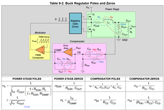
"I guess there is a mistake in the Table 9-2 in SNVSB32B.
According to equation 82 in SLUP340 the first pole of compensator network is defined by RFF (RC2 in SNVSB32B) and CFF (CC3 in SNVB32B). But in SNVB32B first pole is defined by RC1 and CC2.
According to equation 83 in SLUP340 the second pole of the compensator network is defined by RCOMP (RC1 in SNVSB32B) and CHF (CC2 in SNVSB32B). But in SNVB32B first pole is defined by RC2 and CC3.
Table 9-4 in SNVSB32B also includes wrong equations for calculating CC2 and RC2.
Excell Calculator for this chip calculates this components correctly by the way."
We will be thankful for your response.
Kind regards,
Gerald

-
Ask a related question
What is a related question?A related question is a question created from another question. When the related question is created, it will be automatically linked to the original question.