This thread has been locked.

If you have a related question, please click the "Ask a related question" button in the top right corner. The newly created question will be automatically linked to this question.

LM25149-Q1: Question about MOSFET drive capability

Part Number: LM25149-Q1

Hello Team,

I got some questions from customer about LM25149-Q1.

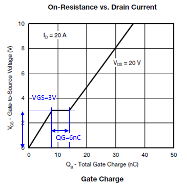
Q. Customer want to use MOSFET(Qg=46nC) and want to output Iout=23.5A. In that case, how much bootstrap capacitance is needed?

Q. The charge of bootstrap capacitor consume during the HS-FET is ON. Can the bootstrap capacitor re-charge fully during the period of minimum Off time?

Q. When VIN=4V, how much gate voltage become?

Q. When customer use Qg=46nC MOSFET, how much time of "turn-on" and "turn-off"?

Thanks,

Yuta Kurimoto

  • As additional information, Customer usecase is as below.

    ・Vin=4V~36V(Load dump)

    ・Vout=3.3V

    ・Iout=23.5A

    ・Fsw=500kHz

    Thanks,

    Yuta Kurimoto

  • Kurimoto-san,

    0.1uF boot cap is fine. No problem recharging during the off time. At low Vin, use a low drop Schottky boot diode to maximize the gate drive rail (which will be ~3.6V when Vin = 4V). The FET should have a low Miller plateau so it can switch adequately at such low Vin.

    Note you can use the LM25149-Q1 quickstart calculator to review power losses and efficiency performance.

    Regards,

    Tim

  • Hello Tim,

    I got additional question from customer.

    Q. How much output voltage of HO pin during output Hi?

    The datasheet says the VCC to CBOOT voltage will be 0.8V at ICBOOT=20mA, But customer can't understand how much output voltage the HO pin become.

    Thanks,

    Yuta Kurimoto

  • Kurimoto-san,

    The boot diode drop should decrease as the boot charge current decreases, meaning the boot cap voltage increase. Also, it may peak charge slightly as SW goes low during the deadtime. Ultimately, the boot rail will be in the range of 4.5V to 5V.

    Regards,

    Tim

  • Hello Tim,

    Sorry for asking again about previous question.

    Q. When customer use Qg=46nC MOSFET, how much time of "turn-on" and "turn-off"?

    Is it difficult to estimate the rough value of turn-on and turn-off time at such low Vin? Customer would like to get the value(Roughly estimation is ok)

    Thanks,

    Yuta Kurimoto

  • Additional information.

    The P.N. of MOSFET which Customer plan to use is SQJ858AEP.

    Thanks,

    Yuta Kurimoto

  • Kurimoto-san,

    The Qg of this MOSFET at Vgs = 5V is 20nC.More important for switching times is the Qgd of 6nC.

    More specifically, during the switch voltage transition, the gate voltage of the FET is clamped at the Miller plateau of (~3V for this FET), so there is ~2V of overdrive. This is applied across the effective series gate resistance, where Igate = Cgd*dv/dt = (5V - 3V) / 3.5Ohms = ~0.6A (allowing 0.5Ohms for the gate driver and including the internal Rgate of this FET = 3 Ohms).

    0.6A into 6nC gives a dv/dt of 0.1V/ns, so a typical voltage rise time for a 12V input is approximately 120ns.The result is this is a very slow FET given the high Rgate (should be ~1 Ohms) and the somewhat high Qgd for this Rdson level.

    Regards,

    Tim

  • Hello Tim,

    Let me confirm my understanding.

    > More important for switching times is the Qgd of 6nC.

    Q. Does the 6nC means below?

    > Igate = Cgd*dv/dt = (5V - 3V) / 3.5Ohms = ~0.6A

    >  (allowing 0.5Ohms for the gate driver and including the internal Rgate of this FET = 3 Ohms).

    Q. Does the 5V means below?

    Q. Does the "Rgate of this FET = 3Ohms" means below?

    Q. Does the "0.5Ohms for the gate driver" means below? In my calculation, should it be 0.08V/100mA=0.8Ohms?

    Q. For the turn on time calculation, My understanding is Q=it, t=Q/i=6nC/{(5V-3V)/3.5Ω} = 10.5ns. I think 120ns is too slow. Is my calculation correct?

    >0.6A into 6nC gives a dv/dt of 0.1V/ns, so a typical voltage rise time for a 12V input is approximately 120ns.

    Q. It would be helpful if you can explain why 12V conversion is needed

    Thanks,

    Yuta Kurimoto

  • Kurimoto-san,

    Your calculations look correct as I made an error in the last step. These are the calculations for the voltage transition time. There is also a current slew rate related to the transconductance of the FET (the current transition time is typically less than the voltage transition time).

    Regards,

    Tim

  • Hello Tim,

    No problem. Customer said appreciation to you that you showed detail calculation procedure. Then they finally got correct value.

    So Let me close this question.

    Thanks,

    Yuta Kurimoto

  • Sounds good - thank you!