This thread has been locked.

If you have a related question, please click the "Ask a related question" button in the top right corner. The newly created question will be automatically linked to this question.

UC3843: A wide voltage output flyback with UC3843

Part Number: UC3843
Other Parts Discussed in Thread: UC3825

Hi ,Have a good day.

we got a special power requirement that we hope to complete a flyback power supply with a wide voltage output to achieve adjustable output from 0V-250V, and the maximum power is 120W.

In order to achieve a very small ripple voltage, we hope to avoid entering burst mode on all output voltages,and we chose the UC3843 and we designed the Demo board.

To meet  more precise voltage and current control,we put the IC on the second side realized by photoelectric driver and current transformerto .

And we found some questions may need your professional support:

1,Can UC3843 meet our needs not to enter Burst mode? Are there other TI ICs that can be supported? 

2,I found that the other companies have implemented this requirement by a flyback with UC3825. Is there any special difference between UC3825 and UC3843 for Burst mode?

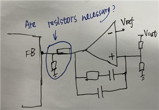
3,We found that our demo board has irregular driving problems. What are the reasons for this problem? We posted the schematic.

4,How should the transformer be designed for this requirement, could you send me your opinion?

Thanks a lot.Flyback.pdf

  • Alvin,

    The general purpose PWM  (GP PWM) controllers you are considering do not have burst mode operation. There is a situation that can arise where pulses are randomly skipping, giving the appearance of burst mode but here's the difference: 

    Pulse skipping (Burst Mode) vs pulse missing:

    A controller that has true pulse skipping  (burst mode) would do something analogous to switching at a minimum duty cycle and then skipping every nth pulse. Some controllers even change to hysteretic mode to implement burst mode. There are different ways to accomplish this but it's done intentionally and in a controlled manner so that the output stays in regulation. Pulse skipping will also impact output voltage ripple but again, this is done in a controlled and predictable manner.

    When the COMP voltage of a GP PWM falls below the minimum threshold, pulses will stop until the COMP voltage returns. This is uncontrolled and results in erratic output operation. Pulses are randomly missing as opposed to periodically skipping. The random missing of pulses can even appear periodic under certain operating conditions.

    Gate Drive and Loop Stability:

    Your demo board has "irregular driving problems"...any number of things could be the cause? Start with your current sense signal seen at U301, pin 3. I don't see a series resistor between the CS resistor (R313) and the filter capacitor C305 - how does the signal appear, is it smooth, no leading edge spike, well filtered and stable? How about the control loop stability over the targeted range of VIN, VOUT, IOUT? Start with a large capacitor in the EA feedback, make C306 =100 nF to start which will give poor regulation and poor dynamic response but will keep the voltage loop stable while you adjust the CS signal and slope comp. Once the current loop is stable go back and adjust C302, R302, C306 to achieve a stable voltage loop. How about your opto driver - is C399 connected directly between pins 8 and 5? Under some condition where the gate drive is stable, what does the pulse look like when measured directly at Q301 VGS? How does this pulse compare to what is measured at U301, pins 6-5?

    Please download and try TI Power Stage Designer so you can quickly simulate what the power stage should see over the full range of your target operation. You can also simulate the control loop with this tool and it runs local on your PC. Good luck with your design and thanks for connecting through E2E.

    Steve M

  • Hi Steven,

    Thanks so much.

    As long as the GP control has a reliable signal and a stable control loop, it can avoid entering the Burst mode, right?

    In addition, there are several other questions that need your help:

    1、 Are the resistors necessary in the posted picture below:

    2、About slope Compensation,under what conditions do we need a series capacitor(Cramp)?

    3、Is there any other more suitable controllers for our application?

    Thank you.

  • Alvin,

    The condition where you could encounter pulse skipping (burst mode) is during low error voltage, in the RAMP valley. To avoid this, you would need to add a DC offset voltage just high enough to lift the error voltage away from the min RAMP valley.

    As far as the resistor divider following the external voltage EA, I would leave those as placeholder in case they are needed. When you use an external op amp, you may need to divide down the output according to the bias voltage applied to the op amp. These resistors help to adjust the op amp output error voltage to be within the dynamic range the FB can respond to.

    The Cramp in the slope comp circuit can be removed if you want. It is in place to block any DC offset that might be seen at the CS signal. I believe it's a good idea to keep it but many design do not use it at all. Also, if you decide to keep it, be informed the circuit you copied has an error and needs an additional resistor to provide a path for Cramp to discharge as shown below (I've entered a request to correct the error in our documentation):

    This is the traditional method for implementing slope comp (with the Cramp DC  blocking cap)

    Regards,

    Steve M

  • Hello Steve,

    How to add a DC offset voltage?Could U share the simple circuit please?

    Does the circuit cause the output voltage to be inaccurate?

    Thank you very much.

  • It should only be required if "burst mode" is encountered. Any DC offset that is added will decrease the dynamic range of COMP.