This thread has been locked.

If you have a related question, please click the "Ask a related question" button in the top right corner. The newly created question will be automatically linked to this question.

BQ769142: Basic test setup for BQ769142

Part Number: BQ769142

Hello,

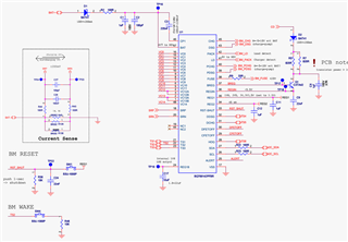
I've a PCB designed for BQ769142 battery manager. I completely followed the TI reference design for connections. At first test, I just wanted to see REG18 output (1.8V internal regulator), and REG1 and REG2 outputs to be sure about working the chip. Then, I just mounted a few elements on my PCB.

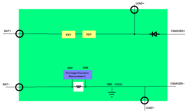
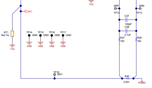
I left almost all pins open (VCx, DSG/CHG/TSx...), just connecting VBAT, CP1, VSS, SRP/SRN, and REGIN-BREG-REG1/2/REG18 (like reference design with their caps, diodes, transistors,...). I connected VBAT to a power supply. Then I started to increase it from 0V to higher values. I noticed that when I reach to around 10V, REG18 is increasing upto 4V, but by datasheet it should not!. REG1 and REG2 are also increasing. BREG is not 5.5V. In VABT around 20V it seems the chip is damaged permanently. I burned 2 chips like that.

What I have done wrong? What is the simplest basic way to see the chip working, like seeing REG18 output, having charge-pump working on CP1... without really connecting it to a multi-cell battery?

Thank you very much

  • Hi Hamzeh,

    It seems like something must be really wrong with your board or connections if REG18 is not showing 1.8V. Do you have anything else connected to this pin besides the capacitor?

    Can you share your schematic?

    Regards,

    Matt

  • Hi Matt,

    The connections are as below. I also attached the full schematic in PDF. I tried to keep everything not-populated as I can (all VCx,TSx, FET enable pins...).

    8255.BMS_sch.pdf

    Thanks

  • Hi Hamzeh,

    Matt assigned me to this issue since he will be out of work this week. I took a look at the schematic and compared it to the reference, but there is nothing that stands out as wrong with your schematic. One suggestion is that if you are seeing a high voltage at BREG above the max rated voltage, this will for sure break the part. A high voltage can occur here if your BJT (Q1) is shorted. This will cause the voltage across BREG to be the same as the voltage at CD which will increase as VBAT increases. You can start here to see if this may be your problem. Also, if the BJT happened to be replaced wtih a pnp instead of an npn, then this will also cause you issues.

    Another thing I noticed, was in your current sense portion of the schematic. It appears that you have connected ground to the SRN side but it should be connected to PACK-. This is not the problem to your issue, but it is important to connect this properly for when you have higher currents. 

    I also wanted to make you aware of your labelling in your schematic. The BM_LD and BM_PACK labels appear to be switched based on pin names. This wont cause any problems since they both go to the same place, but it may cause confusion. 

    Additionally, would you happen to see any other parts of your board that may be an issue: shorts, missing ground?

    Hope this helps.

    Best,

    Andrew

  • Dear Andrew,

    I made another test. I connected BAT+, CAP1, BAT-, GND and current sens resistors, all simulated battery cells (a series of resistor divider. Previous time all cells were open. I don't know open cells can cause a damage or not?!) , and pull-downed RST_SHUT. I kept everything else unconnected and open, even REGIN and BREG. This time I got REG=1.8V correctly with BAT+ = 20V, I got 30V on CAP1 charge-pump. Tomorrow I will carefully check BREG voltage and my transistor, and if everything is correct, connect REGIN and BREG. I hope everything goes well. I guess I first need to enable BREG with host u-controller and then write OTP.

    Regarding the GND, thank you to point this as I have ambiguity there: on positive line, I have BAT+ on one side, and LOAD+/Charger+ (PACK+ is an alternative naming?) on another side, where FETs are there. On negative side, I have BAT- on one side, and LOAD-/Charger- (PACK-?) on another side, where only current sens is in between (then SRP->BAT-, SRN->LOAD-). referring the TI reference designs, I was a bit confused to where should I connect digital GND (VSS in TI), to BAT- or PACK-. There are net-ties on TI ref. design to connect VSS to both BAT- and PGND(PACK-).
    In picture I try to show my configuration. Did I miss anything?

    Thank you very much.

  • Hi Hamzeh,

    Glad to hear you were able to get REG18 working. For REGIN and BREG testing, I found BREG to be about 6V and REGIN to be about 5.59V through my working range (I'm limited to a 30V power supply), so hopefully this what you will find. If you start to see these values increasing, reduce your BAT voltage and re-examine your circuit before proceeding. I hope you won't have another burnt chip. Additionally, while you're testing, I'd suggest against setting the OTP for REG0 (OTP has limited writes) and continue to just set the REG0_EN with your microcontroller.

    Thank you for the diagram. That cleared up my confusion. However, yes, unfortunately the TI ref is not too clear with the way they name PGND. VSS  should be connected through NET TIE 1 to BAT- , but not connected to PACK- (in your case Load-/charger-). 

    So based on your diagram, VSS should be moved to the BAT- side with a recommended net tie.

    Hope your tests continue to go well.

    Best,

    Andrew