This thread has been locked.

If you have a related question, please click the "Ask a related question" button in the top right corner. The newly created question will be automatically linked to this question.

TPS51601A: Possible Routing Problem??

Part Number: TPS51601A
Other Parts Discussed in Thread: CSD18502Q5B

Hi:

I am using this part in an MPPT lead acid battery charger in a circuit very similar to the "Typical Application" circuit in the datasheet.

The switching MOSFETS are CSD18502Q5B's and the inductor is a Coilcraft SER2918-103

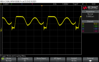
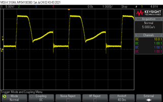
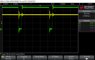
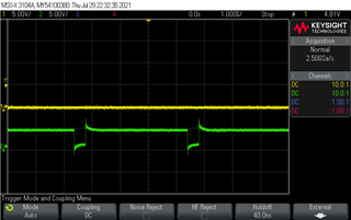
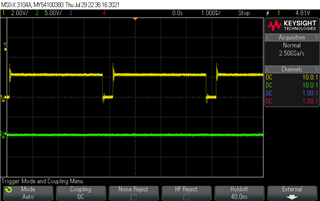
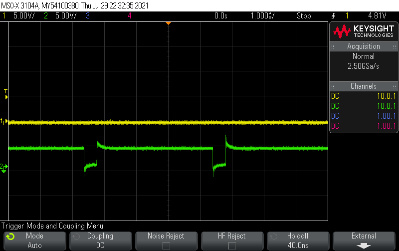
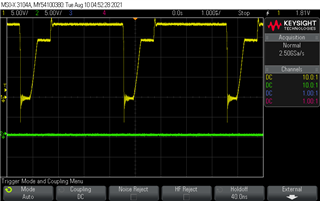
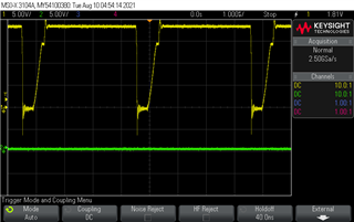
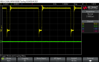
The DRVL gate drive waveform looks great but the DRVH waveform looks as is in the attached scope shot

I routed both with very short wide traces as recommended

Looking for some insight, thanks!

I routed both with very short wide traces, as recommended.

  • Hi Nicholas,

    How did you connect the SKIP signal? It looks like the part is running in DCM so I assume SKIP is low. If you connect SKIP to high, you should see a square waveform (or close to) on DRVH.

    Regards,

    Weidong

  • Hi Weidong!

    I tied SKIP low, thinking that I wanted to be in DCM. I was going by figures 17 and 18 in the datasheet for guidance.

    I will try tying SKIP high and see how the circuit operates

  • BTW, the input PWM duty cycle is 80% in that scope shot

  • Unfortunately, I don't easily have a way to pull skip up to supply. If I let SKIP float will that be sufficient? I don't see an internal pullup or current source on that pin n the functional block diagram

  • When I  tie SKIP to VCC, I get the attached.

  • Attached is a schematic of the circuitP7.pdf

  • Looking at the schematic i supplied, I found that the SW pin is not wired to the node of Q4, Q5 and L8. When I jumper that connection and supply PWM to pin 3, DRVH is held to the voltage across P5 and DRVL is held low. Removing the jumper get me back to what I have above.

  • Hi Nicholas,

    Thanks for the update, yes, this explain the abnormal DRVH waveform.

    Regards,

    Weidong

  • What's weird is that I can easily jumper the missing connection and the part seems to stop working altogether. I verified that I am still supplying a PWM input and double checking my layout for other errors and not seeing anything yet. I also verified in my layout that I have the external pad under the part tied to GND.

  • Also,I was able to solder a jumper to SKIP so I can tie it high or low as needed

  • Are you able to review the schematic and perhaps the layout? Its a pretty simple design so am a bit confused as to what the problem is

  • Hi Nicholas,

    If you already connected SW together between driver the FETs/inductor, then the schematic looks ok. Do you have waveform showing PWM, VIN, DRVH and SA IN?

    Regards,

    Weidong

  • Hi Weidong:

    As mentioned above, I found that the part did not want to operate after completing this connection. What I found was that the DC level on DRVH would simply follow the level on the SW pin despite have a PWM signal appled to pin 3.

    After some experimentation, I found that the part will not start when PWM is applied when a voltage already exists on the SW pin.

    I confirmed this by removing the current sense resistor R122 which removed the battery voltage from the inductor. After doing this, I noticed that the part STILL wouldnt start up when a PWM signal was applied. I then discovered that I needed a bleeder resistor in parallel with the output capacitors C369 and C370 to discharge them and also pull down the net to GND. This allows the part to operate normally.

    I found that, once the part is running, I can then connect the battery to the inductor and the circuit will continue to operate,  delivering current to the battery. 

    I have some ideas to work around this problem for my particular app, the best of which (so far) is to use a MOSFET to isolate the battery from the circuit until the part starts operating, then turn on the MOSFET using a suitable driver

    I realize that this part is targeted primarily for use as the controller in a switching power supply. It looks to me like any voltage that is backfeeding into the output will interfere with the operation of the part. This would include any residual charge on the output capacitors. It seems to me that a bleeder resistor would be required to insure proper operation of this part. In my application, I am deliberately backfeeding a voltage to the part by having a battery connected to (what would normally be) the "output".

    does this make sense?

  • I have this part working pretty well now, except for the startup problem as describe above.

    Any suggestions to work around this? I attached a scope trace showing DRVH (green) and Vout (yellow) once the part is operating.

  • I have some additional findings that I would like to discuss with you  if at all possible. It now appears that I am dealing with a marginal issue with regards to the RC network between SW and BST. I am close to a solution but am in need of some input from someone that knows this part well

    If I cannot resolve this issue, I will be forced to find an alternative solution.

  • I think I have finally isolated my problem down to power sequencing and would like to discuss some possible workarounds when you respond.

  • Hi

    Could you please explain what exactly your find related to the power sequencing and what proposal you have to workaround it? We can review it.

    Regards

    Yihe

  • Hi Thanks for getting back to me!

    I attached a schematic of the circuit if you dont have it.

    If I have a voltage on battery+ before Vcc is applied (or perhaps during Vcc power up) the part appears to lock up.

    If I allow Vcc to power up before applying a voltage to battery+, the part will work reliably. (I should clarify that battery+ powers the rest of the system, including the Vcc power supply (5v)  )

    I found this by breaking the net between battery+ and R122, allowing Vcc to power up and then closing the net. Once the part is powered up properly, I can control it with PWM as expected.

    I am certain that I can work around this problem by placing a MOSFET in line with R122 (immediately before or after it) and bias it on after Vcc comes up. This would require an additional N channel MOSFET that would have to handle full load current (additional heat sinking required) and a driver that could drive the gate voltage high enough to fully enhance it (since the source voltage will be at battery+ which can range from 7v to 15v) such a driver will also require me to add a power supply that can make a Vout of around 15v.

    I think that I can also use a MOSFET in the net that connects the node of Q4, Q5 and L8 to SW. This MOSFET would not need to handle load current but would still require the driver and additional power supply.

    I have some additional testing to do in order to confirm these findings. I would like to get some other ideas on how I can properly power up this part that may be simple are cheaper to implement as opposed to the above.

    2816.P7.pdf

  • >>I think that I can also use a MOSFET in the net that connects the node of Q4, Q5 and L8 to SW. This MOSFET would not need to handle load current but would still require the driver and additional power supply.<<

    I tried a jumper in this net, leaving it disconnected until powering up the part, then connecting it. The part worked properly but the top MOSFET was overheating with just about 1A of current. I think that the long jumper was probably working to distort the signal on SW so not sure if a MOSFET in the SW net would be such a good idea.

  • Hi

    Thank you for sharing this. we will have the right team member looking this and get back to you.

    Regards

    Yihe

  • Anything yet?

  • Hi Nicholas,

    Sorry about the delayed response. Please confirm Skip pin connection. Is it connected to zero or one?

    If connected to zero, then this can be explained by inductor current going to zero and getting into discontinuous mode.

    Best,

    Zhao

  • Hi Nicholas, 

    I will try to help you with your issue.

    Could you please let me know in the schematic what are the voltage levels of the different rails.

    Please send a waveform of the first PWM input to the 51601A. 

    What is the switching frequency.

    Also, what is the purpose of Q15

    Thanks./

    Rama V./

  • PWM on pin 3 (green)

    Fsw is 250 KHz

    Q15 is for reverse polarity protection when the battery is connected to P5

    FYI: Q7 is there to prevent backflow of battery current through the solar array connected to P4 when the solar array voltage < the battery voltage.

    I turn on Q7 when the solar array voltage (sa_in) > the battery voltage (battery (battery+) +2v

    Vcc = 5v

    V (sa_in) is the solar array voltage which can range from 9v to 21v

    battery+ is the battery voltage which can range from 7v to 15v

    Again, if I allow Vcc to come up before applying battery+, (i.e. if I remove R122, power up the 51601 and then replace R122)  the circuit will work perfectly.

  • SKIP pin is tied low as in the schematic.

    >>If connected to zero, then this can be explained by inductor current going to zero and getting into discontinuous mode.<<

    I modified a board so that I could connect SKIP high. This had no effect on my issue.

  • OK. That explains the start-up problem.

    The DRVH works off of a floating supply on BST to SW.

    The cap on BST to SW needs to be charged to ~5V for the start-up. Normally, in low voltage buck converter applications, the output is not precharged and so SW is zero or close to zero. If SW is higher than say 4V or so, the BST cap never gets a chance to get charged for the first PWM pulse. 

    So, any workaround that you do must ensure that the SW node does not see a voltage higher than say 1V or so.

    Hope this helps

    Thanks

    Rama V./

  • This explanation is exactly consistent with what I see in my testing. When the BST cap is charged, the part will work normally. If I discharge the BST cap and try to start the part with battery+ applied (that is, battery voltage on the sw node) the part will not start.

    My workaround is to have a MOSFET either before or after R122 and a 100k resistor in parallel with C370. The MOSFET will be off until after the 51601 is fully powered up and the resistor will bleed off the capacitor charge.

    I can't think of an easier or more cost effective way of holding the sw node low on powerup with out affecting the operation of the part.

    Any suggestions are appreciated.

  • Any recommendations for the SKIP pin?

  • I've included some scope shots of DRVH with a PWM input duty cycles of 70, 80 and 90%

    Should I expect to see this with SKIP tied low? (discontinuous mode)

  • For SKIP pin, I suggest SKIP connected to 5V. This will ensure FCCM. 

    The SKIP low is a feature to get higher light load efficiency provided your controller is variable frequency.

    For fixed frequency PWM, it is better to keep SKIP high. If you want flexibility to study this in the future, you could keep 0 ohm resistors from SKIP to GND and 5V. But start with SKIP tied to 5V.

    Having a MOSFET in series with R122 is a lossy option and not a good idea.

    But you can can use the same control signal that you had in mind to turn this MOSFET in series with R122 and do the below:

    If you can generate a small pulse just before the start of PWMs, you can send the pulse to the Q5 through a simple npn/pnp driver.

    Q5 will turn ON and will charge the BST cap to be ready for switching.

    Note: There was a deliberate reason to design 51601A this way to avoid the turn on of low-side MOSFET (Q5 in your design).

    This is required to support pre-biased start-up of CPUs. But your application is different.

    Rama V./

  • I agree that having another MOSFET in line with R122 isn't the best solution, given the extra power dissipation. I like the idea of briefly pulsing Q5 on, however, this will short across the battery connected to P5 (through R122, L8 and Q5) with a very high current flow and possibly cause a disruptive voltage dip and other potentially nasty consequences.

    I thought about having a MOSFET on the low side of the battery but the grounding won't work out. What I am actually planning on doing is moving the MOSFET Q7 from where it is now to the net "srp". There won't be any additional power loss since I  am not adding another MOSFET and the CSD18502 has a very low Rds(on) when fully enhanced so I can tolerate the small power loss of about 0.4W. I can then use Q7 to work around this issue while it also serves its original function which is to prevent backflow of current from the battery (P5) to the solar panel (P4) when the solar panel voltage is less than the battery voltage.

    What do you think about this?

  • I also confirmed that I do need to have SKIP tied to 5v for this app to work properly.

  • Yes. SKIP can be tied to 5V. It is up to you if you want to have Light load efficiency for future and have an option to tie SKIP to GND also.

    Regarding the start-up issue, the function and connection of the series MOSFET and location is your call.

    But moving it to the srp net means current will be higher as the buck inductor current will be higher than input current and the FET is floating.

    If you want to consider the pulsing the Q5 option, you just need to give a narrow pulse (Similar to normal operating PWM low time).

    That would not increase the inductor current catastrophically. 

    Only thing you should ensure this is done at every start-up cycle and take care of all other fault scenarios etc.

    Rama V./

  • I tried your idea of pulsing Q5 on. If the pulse is kept brief enough (as you mentioned above) the inductor should limit the current flow

    Since I cannot implement a CPU controlled driver circuit on my prototypes, I did the following....

    ... I powered my system with a current limited power supply (current limited to 1A) and used a test lead connected to my +5v supply to very quickly and briefly tap to the gate of Q5 to +5v and almost instantly damaged the 51601. The 1A current limit would have prevented any damage to any of the components in that loop.

    I performed this test before applying PWM. If this test had been successful, the most that would have happened is that I would get up to 1A flowing in the charge loop with the sw node at 0v. If the 51601 had survived, it should have come up working when PWM was applied. 

    I think that the 51601 might not like me driving the DRVL pin to 5v while it is holding that output low. 

    I am also thinking about using a normally closed relay in place of the mosfet and a high value bleeder resistor across the output caps. After powering up, I can briefly energize the relay to open it and then allow it to close. This method works during testing.

  • OK. Please go ahead with the method that works for you. Most importantly, we know the cause of the problem you had originally and a solution.

    However, The 1A current limit on the power supply will not help in the expt you performed.

    The energy into the FET will come from the 2000uF cap.

    Even with say 10V of batt supply, the caps are charged to 10V. 

    So, do the CV^2 calculation and that would be high enough to damage the FET.

    Because a tap with a test lead can be more than few ms whereas a 1-2us pulse can be controlled.

    I leave it upto you the way you want to proceed.

    Let me know if we can close the issue.

    Thanks

    Rama V./