This thread has been locked.

If you have a related question, please click the "Ask a related question" button in the top right corner. The newly created question will be automatically linked to this question.

TPS65185: VPOS is 16V

Part Number: TPS65185

Hello,

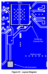
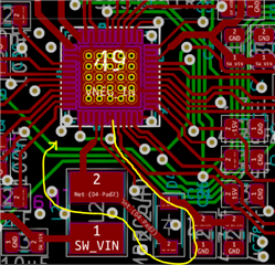
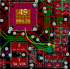
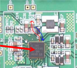
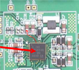
I'm working on a design based on the TPS65185. So far, everything is working well, communication works and all power rails except VPOS have their desired voltage. 
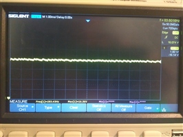
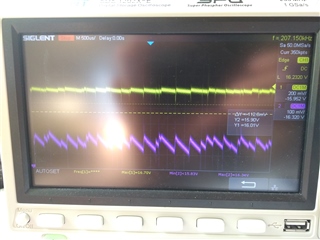
However, VPOS stays at ~16.1V when enabled instead of the target 15V. There is no short with the booster voltage, as the rail is discharged normally when disabled. There is also a small ~0.2V dropout compared to the positive booster voltage.

I tried setting the voltage adjustment register to +/-14.75V or +/-14.25V. While the VNEG rail reacts as expected, VPOS stays at 16.1V. The voltage does not change, even under load. 
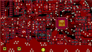
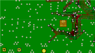
The issue appears on two different prototype boards. 

Some insight and help would be greatly appreciated. Thanks in advance!

  • Hi,

    Thanks for sharing the application schematic - I don't see any concerns. I do some questions to understand this behavior:

    1. Can you measure the boost and VPOS outputs on an oscilloscope? I'd like to see if there are any irregularities in the waveforms. 
    2. You mention the issue appears on two prototype boards. Can you please share how many total boards you have built?
    3. Assuming you have some boards that don't show this issue, can you please remove the PMIC and populate the PMIC from one these two boards that demonstrate the issue? I would like to understand if the behavior follows the device or stays with the board.

    Thanks,

    Gerard

  • Hi,

    thank you for looking into it. I only have the two non-working boards at the moment, and I have tried 3 ICs so far. I am using the TPS65185 instead of the TPS651851 that is used in the schematic, but from my understanding they should be exchangable. 

    I also tried attaching a load of ~500Ohm to the output, which led to a small drop in voltage to 15.9V for VPOS and had no effect on the booster voltage. I plotted the power-up sequence as well, which seems normal.

    The VPOS (LDO1) output is shown on the left, the booster voltage on the right. The only difference I see is the "jaggedness" in VPOS compared to the booster voltage.

    VPOSBooster

    Regards,

    Valentin

  • Hi Valentin,

    You are correct the TPS651851 is a pin compatible higher current option of the TPS65185. Looking at your waveforms, the VPOS (LDO1) output voltage is not expected to be noisier than the boost output. Can you please share the part numbers for C26 and C31? 

    If these capacitors are acceptable we will need to look at their placement in the PCB layout next.

    Thanks,

    Gerard

  • Hi Valentin,

    In your previous response you mentioned "I only have the two non-working boards at the moment, and I have tried 3 ICs so far." Does this mean you've tried 3 different IC's on the same board and this issue was always present?

    I see this is a 25 V capacitor which could have significant derating at 15 V operation. For reference, the capacitors used on the TPS65185 EVM are rated for 50 V. It's possible the capacitor derating combined with the relatively long and narrow 15V trace between the VPOS pin and C31 is creating marginal conditions for the LDO. I don't see this capacitor's DC bias characteristics in the datasheet to confirm the amount of derating due to DC bias - is it possible to get this data from the manufacturer? 

    Thanks,

    Gerard

  • Hi Gerard,

    I have tried two boards each with a new IC, then I swapped the IC on one of the boards, all experiencing the same issues.

    Thank you for pointing out the derating issue, I did not know that this might be an issue. I couldn't find more information except the linked data sheet.
    I'll try to find more suitable capacitors / increase the capacitance to see if this impacts the waveform.

    Regards,

    Valentin

  • I've replaced the caps with two 0603 25V 4.7uF caps, but I see no change at all in the waveform. I'll try to oder other capacitors and another sample of ICs.

  • Hi Valentin,

    To clarify, did you add a second 25V 4.7 uF cap in parallel with the one already on board?

    Additionally, could you take the unit from a board that displays this issue and populate it on a board that doesn't show this issue? I would like to double confirm this is a board issue if possible. 

    Thanks,

    Gerard

  • I added the two capacitors in parallel, for each original capacitor, so 4 in total except of 2.

    As I don't have the EVM, unfortunately I don't have a known working board, so it looks like I'll have to take chances.

  • Hi Valentin,

    Understood - in that case our best indicator of a board issue is to try additional IC samples. Please let us know when you have more samples to test. In the mean time, can you provide additional layout images for the internal and bottom layers of your PCB?

    Thanks,

    Gerard

  • Hi Gerard,

    There are only two layers, where red is the front and green is the back layer. The screenshot doesn't show the ground fills, but the bottom layer is mostly ground fill except for the shown traces. I know that this is not optimal, but I would be surprised if that would cause this specific issue and not issues / noise elsewhere.

    I'll report back once I have different components to try.

    Regards,

    Valentin

  • Hi Valentin,

    At least four layers is generally recommended for power supplies to allow a continuous, dedicated GND plane directly beneath the power components. This ensures a good, low impedance return path for proper regulation, and to minimize noise and EMI. 

    In the case of this deviceI would also like to see the bottom layer to check the thermal pad connection to VN - as shown in the datasheet a copper pour is recommended for power dissipation. On this note, have you read the device registers during operation to determine if any faults/interrupts are present?

    Thanks,

    Gerard

  • Hi Gerard,

    Regarding the registers: I have read the interrupt and power good registers, and no interrupts where detected (at startup as well as after extended on-time). Power good shows power good for all rails. The other registers all have default / sensible values afaik.

    Below are screenshots of the bottom and top copper layers:

    If I have to redesign the board, I guess a 4 layer board will bemore appropriate. 

    Regards,

    Valentin

  • Hi Valentin,

    Understood that no interrupts are indicated. I think the next step has to be testing more units on the application board. Please capture the first startup waveform to confirm that there's no unexpected behavior. If the issue persists on new units then we'll focus on PCB layout improvements, especially around the boost and LDO1. 

    I will add that a VN pour on the bottom layer is recommended for power dissipation. Based on your layout, the only way for the PMIC to really dissipate heat is essentially through the package to the air. Here's an example used on the EVM:

    Thanks,

    Gerard

  • Hi Gerard,

    I've tried with new ICs today, unfortuately the same issue appeared. Hiere are some waveforms of VPOS and the boster rails:
    It looks like the regulator is starting to work, but there is intereference from the booster:

    I assume this is because the booster loop is too large and the VPOS trace too close? I added better capacitors as well. Do you know of any way to test this on an existing board, or do I need to manufacture a new prototype board?

    Regards,

    Valentin

  • Hi Valentin,

    To clarify, CH1 in this picture is the boost output, and CH2 is VPOS, correct?

    Thanks,

    Gerard

  • Hi Valentin,

    Thank for the quick response. Unfortunately, if increasing the LDO output capacitance has been unsuccessful, I can't think of any other board-level fixes we could try. It may be best to start on a new prototype board - please feel free to post again here for schematic/layout reviews. 

    You are correct a large boost loop (the output loop) can create noise spikes in the voltage output. The boost output capacitor is the most important component in the boost converter layout but they are located quite far from the VB pin with narrow traces in this prototype. The discontinuous GND plane on the bottom layer is also increasing the size of this loop (resulting in the shortest loop actually being on the top layer). It's also best practice to route the VB/VPOS_IN/VDDH_IN after the output capacitors. This app note has a great tips for boost converter layout: https://www.ti.com/lit/an/slva773/slva773.pdf

    Similarly, the VPOS output capacitor is located relatively far from the VPOS pin with a narrow trace. In general, LDO output capacitors should be placed close to the IC output pin connected with a short, wide trace. 

    The TPS65185 EVM uses a tight output loop shown below with a continuous GND plane on Signal Layer 1. Note that it also routes the boost output to VB/VPOS_IN/VDDH_IN after the output capacitors.

    The VPOS LDO output capacitor is also placed as close as possible to the VPOS pin (after prioritizing the boost components), with the trace made as wide as possible.

    Please also refer to the TPS65185 EVM for an example of good component placement with this PMIC: https://www.ti.com/lit/ug/slvu548a/slvu548a.pdf

    Thanks,

    Gerard

  • Hi Gerard,

    Thank you very much for your help and writing such a comprehensive reply! I'll make a new board taking this into account.

    Regards,

    Valentin

  • Hi, 

    I've attached a new layout, immitating the EVM where possible. Assuming the presence of a continuous ground plane, do you see any immediate issues with this layout?

    Thanks,

    Valentin

  • Hi Valentin,

    This initial placement looks good. Just a few comments:

    • Connect pins tied to the VNEG_IN net (VCOM_PWR, VNEG_IN, etc.) through internal or bottom layer routing, instead of directly to the thermal pad. The thermal pad can be relatively noisy due to switching activity in the IC.
    • Include a VNEG_IN pour on the bottom layer dedicated to the device thermal pad for heat dissipation.
    • Add multiple GND vias around all power components. This includes input/output capacitors and inductors where applicable. 

    Thanks,

    Gerard

  • Hi Gerard,

    I've done the routing around the thermal pad, however, I'm a bit unsure how to connect the pad to VNEG_IN. Right now,
    I have the thermal pad connected through the PBKG pin as before, but all other connections routed on the bottom. The bottom thermal pad only connects through the thermal vias:

    Is this correct?

    Thanks,

    Valentin

  • Hi Valentin, 

    This is the correct approach. The EVM also has a single point connection from PBKG to the thermal pad:

    Thanks,

    Gerard

  • Hi,
    I got a new revision of boards and the issue has now disappeared. Thank you again for your help.

    Regards,

    Valentin

  • Hi Valentin,

    Great to hear! Please feel free to post on E2E again if you have further questions regarding this or any other TI device.

    Thanks,

    Gerard