This thread has been locked.

If you have a related question, please click the "Ask a related question" button in the top right corner. The newly created question will be automatically linked to this question.

TPS62902

Other Parts Discussed in Thread: TPS62902, TPS629210-Q1, TPS62912, TPS62861

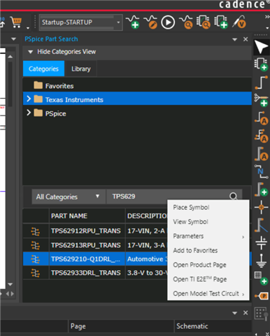
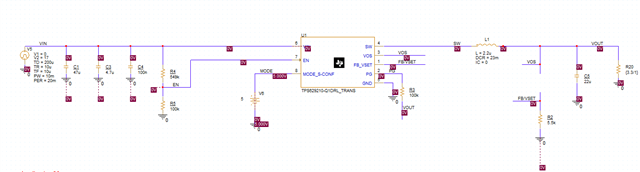
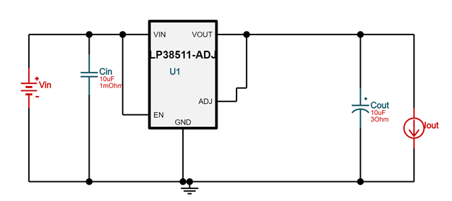
In need to do a board layout where I have multiple different power supplies in 0.5V-2.7 V range. These should be created from for up to four source voltages. I am thinking to use for that TPS62902 DC/DC buck converter. I have to make sure that I get very a good power integrity across the whole board. Some of my components would share the same source voltage. I am wondering how to do that. Shall I simply tie loads to the converter? Is there any limitation on the number of converters I can use for the same source. Should I always use tracking output as an input to the next converter? Is there any other component that can probably suit better? To reduce crosstalking at loads, it seems I should put some inductor bead at the input to the converter.

I should ensure that return currents are also handled properly. The components I use are of quite high frequency going over 20 GHz I see some general guidelines for such things. However, I miss documents that can guide when it comes to placing different components. It will be great if you give me an idea on the above questions and provide me with some guideline and documents.

Thanks
Olonbayar

  • Hello Olonbayar,

    I think the TPS62902 would suit your application well as it can support output voltages in the range 0.4-5.5V. There shouldn't be a problem tying multiple loads to the converter or tying multiple converters to a source voltage given that you are not exceeding the maximum current rating of the device or voltage supply rails. 

    One consideration when powering multiple loads from the buck converter is the additional output capacitance that is added to the input of each additional device to ensure Power integrity. Section 8.3.2 of the datasheet helps address this issue.

    The soft start and tracking can be used if you want to ensure that all the voltages sequence on at the same time or sequentially, but is not a requirement and you can use less external components if sequencing is not critical to your application.

    An inductor bead at the input may help reduce noise, but will also cause a voltage drop from the supply voltage to the input of the buck converter that needs to be handled to ensure the input voltage doesn't drop too low. 

    The datasheet and EVM user guide can provide PCB layout information for your application. Here is also an Application note on layout tips for EMI reduction: SNVA638A .

    Let me know if this helps.

    Thanks,

    Joseph

  • Hi Joseph, 

    Thanks a lot for your replies. This clarifies many points I had. By the way, do you have SPICE model for the component so that I can simualte the converter in LTSPICE. It will be great if you can give me some advices on that.

    When connecting multiple load to one converter, the datasheet says that to the input of each load n X47 uF capacitor should be connected. Does this imply that each capacitor is 47 uF and n refers to the number loads. Or is each input capacitor nx47uF.   

    Thanks for the support

    Olonbayae

  • Hello Olonbayae,

    With multiple loads in this specific example they use a 47uF capacitor for each load where n is the number of loads. Note that they also include some small trace resistance to each load such that an AC signal is still measured on the VOS pin (for voltage regulation). 

    The SPICE model for this part is still in progress, however the TPS629210-Q1 device operates in a similar manner and has a SPICE model, with a 1A current rating instead of 2A.

    Thanks,

    Joseph

  • Hi Joseph, 

    Thanks for your replies. Great. Can you please recommend me ways to use the TPS629210-Q1 spice model? I was trying LTSPICE and could not get it working. I have not much idea about adding the model to LTSPICE. It would be great if you can provide me some hints in doing that maybe link, video or some document from your customers that can help me. 

    Thanks,

    Olonbayar

  • Hello Olonbayar,

    I am not familiar using LTspice, however TI provides a similar tool called PSPICE for TI that is free for download: https://www.ti.com/tool/PSPICE-FOR-TI#tech-docs. The TI libraries will have all the available parts pre-installed so TPS629210-Q1 will not have to be imported. There is also a great wealth of knowledge and resources for learning how to use this tool at the site or can be searched for on ti.com.

    Thanks,

    Joseph

  • Hi Joseph,

    Thanks a lot. It was very usful. I installed PSPICE and tried to simulate a bit. In my installation I could not find the model you mentioned. It is actually very similar to mine would have been nicer if it were there. I found the model for TPS62912 in my installation which is the closest. I still tried to simulate it with the schematic 8-1 from the data sheet. But I could not get it running for a simple configuration. I wanted to simulate DC/DC converter to which multiple load is tied and see if they get the same voltage. For that it will be very appreciated if you could send me the model for  TPS629210-Q1 as it appears very similar to the converter I wanted to use. 

    Thanks in advance

    Olonbayar     

  • Hi Olonbayar,

    The TPS629210-Q1 should be included in the TI part libraries. I would try to reinstall the libraries or look for an update:  
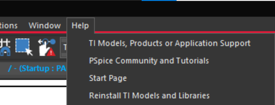
You can reinstall using the Help toolbar.

    If that doesn't work download the model file from: https://www.ti.com/lit/zip/slvmdm5 .

    Then extract the files and add them to pspice through the following:

    1.) Place Part

    2.) Add part library

    3.) Search for downloaded folder extracted.

    4.) Select the .OLB file from the folder

    This should allow you to add the part to your schematic.

    If you are able to reinstall as stated first then there will be a test circuit schematic so you don't have to build a model.

    Go to pspice part search, search for TPS6292, right click on TPS629210-Q1, select open model test circuit.

    If you can't get the model working I can try to send an example schematic for you to try.

    Thanks,

    Joseph

  • HI Joseph,

    great. It helped a lot. I have few inquiries.

    I am simulating using model for component TPS629210-Q1. I did not any change except voltage dividing resistors. 

    It seems I can get the voltages I need which are larger than 0.6V. I change there R1 and R2 according to the eqn. 13 from the datasheet. But if I want to get 0.5 V I should do the setting bit different way using only R2 (Table 8-2, VSET selection table), I am not getting what I expected. I am submitting the circuit diagram. It will be great if you can have a look at the diagram  or run it, and give me recommendations. 

    The other question is if I want to change the input voltage, where should I do this? The model says that it is set to 12V. How can I configure it?

    Thanks in advance

    Olonbayar  


  • Hello Olonbayar,

    I made the following modifications to your setup:

    1) Changed the VSET resistor R2 to 4.87k (0.4V selection)

    2) Replaced V6 with a 34k resistor (select VSET mode based on Table 8-1).

    3) To change the input voltage adjust the V2 parameter of the input voltage step which is currently set to 17V (V5).

    I get the following transient waveforms at steady state.

    Thanks,

    Joseph

  • Hi Joseph, 

    Thanks for your quick replies. It helps a lot. I wanted to get 0.5V for my Vout and for that I set everything as in the previous post. I thought I would get 0.5V by setting resistor value between 4.87k and 6.04k (table 8-2 from the data sheet). This gives either 0.4V or 0.6V not depending on the resistor. Can yon please comment on that? Is there other ways to get 0.5V? 

    Thanks 

    Olonbayar 

  • Hi Olonbayar,

    Using VSET only allows for 0.4V or 0.6V setting and doesn't have a 0.5V setting.

    Also if external feedback is used the lowest you can go is 0.6V (because the VFB pin is regulated to 0.6V).

    It doesn't look like you will be able to achieve exactly 0.5V but only 0.4 or 0.6 at these low levels.

    Thanks,

    Joseph

  • Hi Joseph, 

    Thanks for your reply. I was searching a DC/DC buck converter at your website which can give 0.5 V output and the current around 2A or even less. The converter TPS62861 seems can do it. However it is configured through I2C interface. Is there any other converter with simpler setting that does not require interfaces?

    Should the setting be done with FPGA or other controller? Can we get the example code for FPGAs to do the setting?

    Thanks Olonbayar 


  • Hi Olonbayar,

    Yes it looks like TPS62861 can support a 0.5V output as it is configurable in 12.5mV steps. However, this device falls under a different product line which I am not as familiar with.

    If you want help from experts on these Low voltage products I would recommend putting in another E2E request using this part number so it notifies that product line.

    It also looks like TPS62080x may be a contender for this low voltage application.

    Thanks,

    Joseph

  • Hi Joseph,

    Thanks all for your quick responses. I really appreciate that. 

    I need to get 0.5V. For that I think low drop out regulators could be the simplest to use. LP38511TJ-ADJ/NOPB seems to offer output voltage 0.5 V. I then used webench for the schemtic I can use. I got the following. There is no resistors connected. I am sure if will be fine. It will be great if you have a look at it and do comment.  

     Thanks

    Olonbayar

  • Hi Olonbayar,

    Yes the ADJ pin can be directly connected to VOUT in order to generate a 0.5V output voltage. The one thing I would note is that it appears that Cout in  your schematic is not a ceramic capacitor, this LDO requires at least one 10uF ceramic (low ESR) capacitor near the output of the LDO to operate properly. Below is a screenshot of the datasheet section which discusses this.