This thread has been locked.

If you have a related question, please click the "Ask a related question" button in the top right corner. The newly created question will be automatically linked to this question.

TPS652353: Checking Power Output without Load

Part Number: TPS652353

Hi,

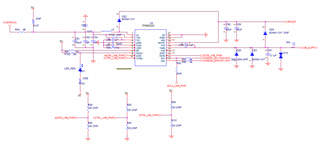
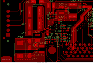
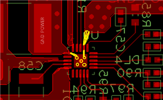
I had earlier requested a design review here for my TPS652353 design.

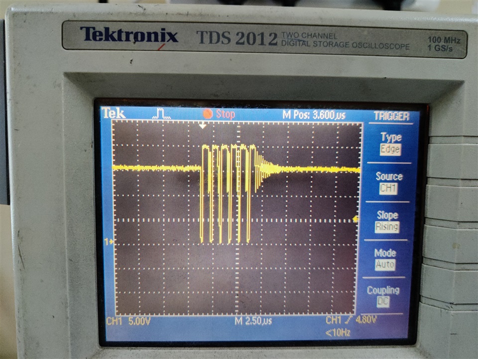
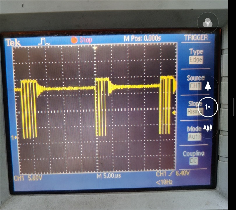
Now my board has arrived and I wanted to check the output voltage by setting it through I2C.

My input voltage is 5 Volts, I have connected VCC and VIN pins together as per  the datasheet.

However, when I check the output with DMM it is at 3.2 Volts always.

I checked the status register and CABLE_GOOD  and VOUT_GOOD are low.

Is it the case that without a proper load like an LNB or dummy load the voltage will not be set?

  • Hi, Mohit 

    1. Could you send me the schematic again? and could you send me the layout file? layout screenshot is ok.  

    2. What is the DMM? and what is the loading when connected with DMM? 

    If remove DMM and no loading, what will Vout be? 

    3. Could send me the Vout and LX waveform? 

  • Hi,

    This is the schematic portion of the LNB Power supply.

    I will send rest of the things tomorrow.

    I checked with default mode as in the schematic and 15V input and the IC and surrounding area got heated up. It was taking around 350mA without any load from the 15V supply.

    EDIT: This is the screenshot of the layout. I can send the Layout file on DM if required.

  • Hi, Mohit 

    1. I review the schematic, it is ok. 

    But I found some errors in the layout. 

    a. please place more VIAs on thermal pad. b. please make PGND trace wider. c. the LX trace looks narrow. 

    Some questions: 

    1. Is Vout normal when not connecting DMM? (at no loading). If yes, could you add loading? and increase loading to max gradually until issue happens.  

    2. Could you send me some waveforms of Vout and LX when issue is happening? including zoom in and zoom out waveforms. I suspect IC trigger OCP and work in hiccup mode, so i want to check the hiccup on/off time. 

  • Hi,

    Thanks for the response. I will implement your layout suggestions in the design. I do not understand why or how but today the IC is behaving OK and giving out expected outputs. The current from 15V supply without load is around 7mA and there is no heating. 

    Not sure what was the issue before.

    I have attached LX pin waveform just for reference.

  • Okay, the waveforms look normal. 

    Once you can duplicate the issue, please send it to me for analysis. 

  • Hi again,

    I have a different issue now. I connected the output of the IC to a 50 ohm dummy load (rheostat) with 18.2V output.

    The current rose to the maximum set by me(1.5A).

    So. I switched it off and the no load current changed to 80mA from 7mA which I was seeing earlier.

    Also, now when i set the output to 18.2V by i2c, i get 19.6 volts at output.

    When i set is to 13.4V, i get 17.4V. this is the state of LX pin now. The VCC pin reads 6.4V.

  • Hi, Mohit 

    1. Output current rose up to 1.5A? I saw Riset is 110kohm, the Iout should be limited to ~1A, IC cannot output 1.5A, do you have waveforms? 

    2. If change Vin to 12V, set Vout by I2C, please check if Vout is normal or not? 

    It looks IC was damaged in the test of connecting 50ohm dummy load.  

    All of boards have this issue? 

    3. Remove DZ4, and check again. 

  • Hi,

    1. I was measuring the output current of the power supply from where I was supplying the 15V. I couldn't check the output current of the IC.

    2. When i set VIN as 12V, when I give 18.2V command i observe 19.2V at the output and when I give 13.4V command I observe 17.2V at output.

    Is there a reason you can think of why the IC would be damaged in this test?

    Right now I do not have another board.

    Edit: DZ4 is not mounted

  • Hi, 

    1. Ok. 

    2. I thought 1.5A might damage IC. if 1.5A is input current, i think it is no problem. 

    3. Could you double check the Vout I2C setting command? make sure it is correct. 

    4. Could you optimize the layout? especially make the GNDP/GNDA trace wider which can reduce the parasitic R on GNDP/GNDA trace.  

    Maybe you should solder off the IC, then optimize layout, and re-solder IC on. 


  • Hi,

    The IC was earlier taking 7mA from the 15V supply input, but after the incident of taking 1.5A with load, it has started to take ~80mA.

    So I suspect something has gone bad in the IC.

    I will get it replaced, but what I am concerned about is why should a 50 ohm load change the current so much . 50 ohm load should take around 0.36 amps at 18.2V, which comes to around 0.44amps at the 15V source.

    The command is same as the one which I used before.  I have not reprogrammed my microcontroller which is giving I2C commands to the chip.

    I cannot make the trace wider right now, the pcb will be required to be redesigned.

    I will get it redesigned but I need to make sure that there is no other issue before that.

  • In layout, GND trace is narrow which has big parasitic L and R, so with 50 ohm loading, when switching, they will cause big bouncing noise on LX which might make IC bad. 

    So suggest replace a new IC and test again. 

  • Ok.

    I will try again with new IC and get back soon. Thanks for the support