This thread has been locked.

If you have a related question, please click the "Ask a related question" button in the top right corner. The newly created question will be automatically linked to this question.

TPS27SA08-Q1: What does affect retry time?

Part Number: TPS27SA08-Q1
Other Parts Discussed in Thread: TPS27SA08

Hello,

I have a question concerning retry timing (t_RETRY).

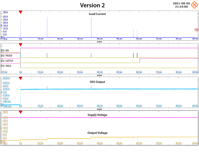
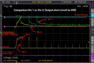
I build a PCB using TPS27SA08-Q1. Testing has been succesful and the retry timing was as expected and as stated in the datasheet (page 9): arround 2ms. That was perfect for my usecase.

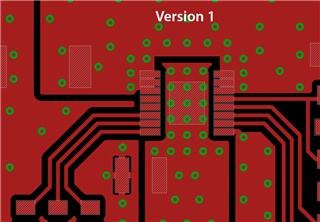
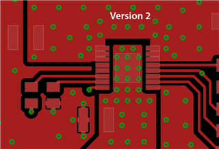
Now I made a new revision of the board and trace layout arround TPS27SA08-Q1 is nearly identical. So thermal coupling should not be an issue. But with this new revison retry timing is completely different. Arround 30ms sometimes even longer. Unfortunately this is not an acceptable time :-(. What could cause this changed behavier? I even replaced the TPS27SA08 to make shure it is not a faulty part. For nearly two days I am resarching for the cause but no luck ...

Any help or ideas would be greatly appreciated.

Thanks a lot an regards,

Bernd

  • Hi Bernd,

    The retry time should not change. The retry time can be though of as a deglitch time. It is the minimum time the device waits to turn on after a fault state has been hit. Depending on the fault state, the actual retry event can happen much later than the retry time since the fault may not have been cleared.

    A good example of this is thermal shutdown. If the ambient temperature of operation is high, then it might take longer than the retry time for the junction temperature to drop below the hysteresis threshold. Figure 9-5 on the datasheet is a good example  of this behavior. The device will only auto-retry after the following conditions are met:

    1.  All faults have cleared

    2. Retry timer has expired

    3. Latch pin is low

    4. EN pin remains high

    Thanks,

    Shreyas

  • Hi Shreas,

    thanks for your fast answer. All the conditions concerning pin states (EN, LATCH, …) temperatur, supply and load are identical in my first and second design. So there is the question why does it behave so different?

    Regards Bernd

  • Hi Bernd,

    What is the failure event that is being tested here? There is a chance that the fault state is not being cleared in your second design. Is this behavior consistent over multiple devices? A good test might be to swap the device onto your first design and see if the behavior is limited to the device or to the design.

    It would be helpful if you can also provide scopeshots of the failure event from the first and the second design for us to compare performance. 

    Thanks,

    Shreyas

  • Hi Shreyas,

    here are some pictures of what's going on. The load is an DC/AC Inverter (24VDC to 230VAC) with a very high inrush current. All surrounding conditions are pretty much identical (as far as it is controlable ;-))

    Thank you and regards

    Bernd

  • Could the quality of the solder joint on the exposed pad affect thermal behavior in case of overcurrent/shortcircuit? As I understand the shutdown in case of overcurrent is a matter of raising junction temperatur (am I right?) But I suppose, because the time to react to overcurrent is pretty fast, this measurement of temperature must be done internally and could not (or not very much) be affacted by the copper planes the device is soldered to. I think it would be much slower then. Do you know what I mean?

    Regards
    Bernd

  • Hi Bernd,

    From what I am seeing this looks to be a repeated current limit fault as evidenced by the foldback.

    The mechanism of current limit in this device is that once the device recognizes the fault, it modulates its resistance to hold current at the defined level. This results in large power losses across the device which eventually lead to device shutdown from thermal protection. For the thermal fault to clear, the junction temperature has to drop below the shutdown temperature by a defined t_hyst (hysteresis). Until this condition is met, the fault state on the device does not clear.

    Good thermal connection between the thermal pad (VBB pad) and the board is essential here. The major heatsinking pathway of the device is to the board through this pad. If there is incomplete solder here then the junction could take longer to cool down that what is expected. From your testing, you can see that the device is recognizing the fault but is not restarting after a long time. I think this points to a slower dissipation of the thermal energy. As mentioned, a good test is to take one of these device from Version 2 board and put it on the Version 1 board. This will confirm if the device itself is exhibiting a incorrect behavior or if the issue lies with the heatsinking capabilities of the board. Another option is to do this test using an EVM which you can acquire from our website. 

    Thanks,

    Shreyas

  • Hi Shreyas,

    thank you very much for your detailed and very informative answers. Now I'm getting a deeper understanding of the part.

    I will try to investigate further concerning the soldering of the part. Since these boards ar prototypes I solder them by hand (using a preheater plate and hot air) So the soldering of the exposed pad has some sort of uncertainty. Also I will try to swap the part from version 1 to 2.

    From your experience what would you say: Is the behavior of version 1 that what should be expected?

    Thanks again,
    Bernd

  • Hi Bernd,

    With the information at hand, both can be acceptable behavior. From what I am seeing, the device correctly turns on, recognizes the CL, tries to current limit, heats up and then shuts down. Once the temperature of the junction has dropped, the device retrys. After unsuccessful retrys, the device folds back the current limit as expected. 

    Before desoldering the device, I would recommend retesting Version 1 and Version 2 but set up the device to measure junction temperature.

    The SNS mux internal to the device can be configured to output a voltage corresponding to junction temperature. This may help us understand if the junction is remaining warm for longer time on Version 2.

    Thanks,

    Shreyas

  • Hi Shreyas,


    sorry for the delay in answering back. I was very bussy these days and therefor had no time to further investigate the issue. But today I did some new measurements.

    Observing the temperatur is a very good idea - didn't think o it yet.
    I did so and found, that the temperature in Version 2 is behaving nearly the same as in Version 1. Temperatur rises, device shuts off -> temperature drops (in a pretty similar slope and time in both versions)  -> Version 1 retrys after about 2ms, Version 2 does not for serveral 10ms (devicve temperature here dropped meanwhile to room temperature) until retry. So if it is not that the temperature/cooling down is making the difference I am quite back to the starting point ... scratching my head. What else could cause this long delay until retry?
    I attatched a picture where I overlayed the two versions in Photoshop ...
    Thanks a lot,
    Bernd

  • Hi Bernd,

    Thank you for your detailed picture. I think this shows us a very interesting phenomenon as both designs sufficiently cool down. 

    By any chance have you completed the test that involves swapping the devices from Version 1 to Version 2 and vice versa? This would confirm if the device is experiences an issue or if the issue is cause from the board.

    Please feel free to also loop in your TI field/sales representative as well as myself to continue this discussion over email. 

    My email is s-dmello@ti.com.

    Thanks,

    Shreyas