This thread has been locked.

If you have a related question, please click the "Ask a related question" button in the top right corner. The newly created question will be automatically linked to this question.

UCC27517: Correct connection to drive 2 MOSFET by 2 UCC27517

Part Number: UCC27517

Hi Team, 

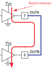
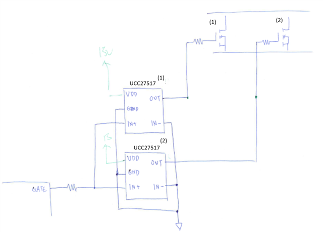
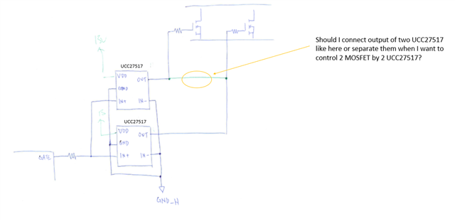
My customer wants to know should they connect output of UCC27517 together or not when driving 2 MOSFET by 2 UCC27517,

could you kindly help confirm it and let me know the reason of your answer? Thanks.

Please let me know if you need more information from customer. 

Regards,

Jo

  • Hi Jo,

    Thanks for reaching out!

    -------

    They should not do it, because if there is any mis-match in timing between the two drivers, there will likely be shoot-through, damaging the output stages of the IC's.

    To ensure the two power FETs turn on as close as possible to the same time, the input signal trace should have a symmetrical / equal-distance path to each of the input pins.

    If the customer wants me to review their layout design, please feel free to let me know on E2E in the future!

    -------

    If this makes sense and I answered your question, please press the green button.  Otherwise, please feel free to follow up!

    Thanks,

    Aaron Grgurich

  • Hi Aaron, 

    Thanks for explaining the reason. Let me double-check, so following connection is correct if customer wants to control two MOSFET by two UCC27517?

    Regarding following statement, let me double-check.

    Do you mean the trace between "UCC27517(1)'s output to MOSFET(1)'s gate pin" and "UCC27517(2)'s output to MOSFET(2)'s gate pin" should be symmetrical and equal-distance?

    To ensure the two power FETs turn on as close as possible to the same time, the input signal trace should have a symmetrical / equal-distance path to each of the input pins.

    Thanks.

    Regards,

    Jo

  • Hi Jo,

    Yes, this is schematic is correct.

    -------

    The customer should also locally bypass each of the drivers with at least one 1uF capacitor directly across the VDD and GND pins.

    But to be safe, they should bypass each driver with a 0.1 uF capacitor as close as possible to the VDD and GND pins and a 1 uF capacitor next to that.

    Both the IN+ traces need to have the same length, and both of the OUT traces need to have the same length as well.

    Also, the customer will want to make sure the driver is very close the the power FETs as well to minimize the current loop to the gate of the FETs.   Consider looking at the "Layout" section of the datasheet.

    -------

    If this makes sense and I answered your question, please press the green button.  Otherwise, please feel free to follow up!

    Again, if the customer wants me to review their layout design, please feel free to let me know on E2E in the future.

    Thanks,

    Aaron Grgurich