This thread has been locked.

If you have a related question, please click the "Ask a related question" button in the top right corner. The newly created question will be automatically linked to this question.

UCC2897A: Active Clamp Forward with Sample Start Issue (UCC2897A)

Part Number: UCC2897A

Hi all,

I use the IC UCC2897A to do High-side Active Clamp Forward Converter.

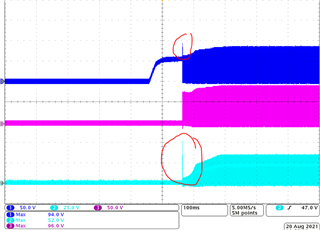
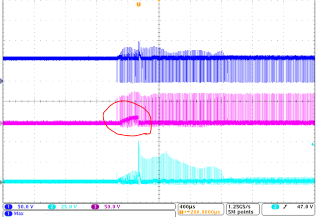
In the sample start-up. Have a peak voltage in the Secondary side Mosfet -Vds (SR1).

The sample is OK. Output Voltage is right.Only in the sample start-up.Have a peak voltage.

I use the IC UCC24612-1 in Secondary side SR.However, I use the Schottky diode have the same issue.

What's wrong in it? I have put snubber in SR,But continue to have the same problem.

This peak voltage only appeared after the S1 switch signal came out, not the first signal.

Thanks!

note: fig.1 picture is from google

Ch1: S1-Vds  Ch2:SR1-Vds  CH3: S2-Vds

  • Hi Micky,

    I see the spikes.  I will need additional information to find the root cause.  If you could email me (e-reicher@ti.com) the detailed schematic for the UCC2897A, the transformer, the MOSFETs, and the UCC24612-1 that would be most helpful.  Once I have the full schematic I can consult with the active clamp forward experts here at TI.  Also, when does this spike occur, as VIN ramps up?

    Regards,

    Eric

  • Hi Eric,

    Due to customer relations, it may be inconvenient to provide detailed circuit diagrams. I use the High-side active clamp forward.

    Vin is 30Vdc - 55Vdc, Vo is 12Vdc. The transformer turn ratio is 7:6. The s1 and s2 mosfet is FDMS86200/ON. Clamp cap is 0.4uF. The SR1 and SR2 is BSC070N10NS5/INFINEON. The IC peripheral circuit is the same as the recommended circuit in the specification.

    when does this spike occur, as VIN ramps up? 

    I'm not sure what you mean. It will only appear at the moment of booting, regardless of the size of Vin at this time.

    However, one thing can be found in the picture. This peak voltage will only appear after the S2 switch is raised. I am not sure why the S2 switch will rise. It should not be correct under normal operation. Do you have any opinions? thanks!

    Regards,

    Micky

  • Hi Micky,

    Thank you for the reply.

    You mentioned using high-side active clamp circuit and N-Channel MOSFETs for both S1 and S2.  It's difficult to troubleshoot an issue without a detailed schematic.  However, there is a very good Application Note dedicated to high-side active clamp and gate drive.  See, sections 4, 5, and 6 in the following link.

    https://www.ti.com/lit/an/slua322/slua322.pdf?ts=1629728220529&ref_url=https%253A%252F%252Fwww.google.com%252F

    Regards,

    Eric