This thread has been locked.

If you have a related question, please click the "Ask a related question" button in the top right corner. The newly created question will be automatically linked to this question.

TPS62912: Achiving ultra low noise

Part Number: TPS62912
Other Parts Discussed in Thread: TPS62913

Hi,

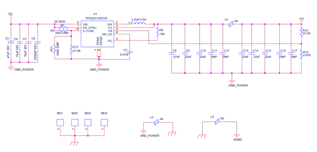
Using Webbench i ended designing a low noise power supply as shown below

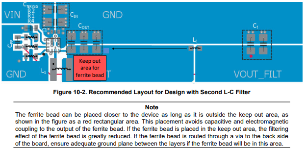
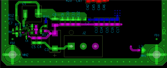
below is the screenshot of the layout - Routed as per guideline and with in top layer completely

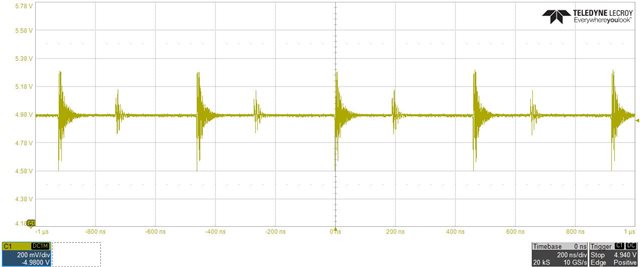
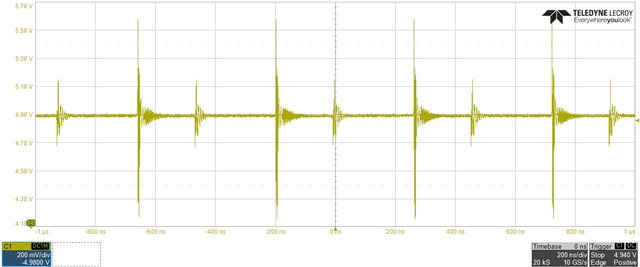
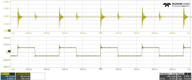
but when i measured the noise i ended up seeing a ringing noise arround 500mv, kindly help in reducing the noise as said in the product description of TPS62912 which is whooping -20 µVRMS

How to Achieve such low noise, which is very cricitcal for my design as of now.

  • Shyam,

    Thanks for your question. Have you measured the ripple on a standard EVM, and built the design using your components on the EVM? 

    Can you detail how you are measuring the output ripple?  Where you are measuring, and how you are measuring?  If you are using a standard probe with a long ground loop, or are using tip and barrel technique across an output capacitor?

    Can you send a picture of the output voltage ripple along with your measurement technique?

    Looking at the layout, it seems you have rotated the device and the output inductor 180 degrees, and have not followed the layout recommendation in the datasheet at all. The VO trace length needs to be kept very short, as shown in the example layout, and your layout has this wrapped around the inductor. 

    Please let me know if you are able to measure the lower ripple on an EVM, and send your results.  Thanks.

  • Above is the Noise across last capcitor and PGND, measured using tip and barrel technique

    below is the noise after a filter across the sensor bias, across AGND and pin 2 of sensor pin(photo diode sensor not mounted)

    filter for sensor bias is as below

  • Thank you for the waveforms of the output.  This appears to be SW node ringing, and not output ripple due to ESL, ESR, or trace inductance. Are you able to use a TPS62913 EVM and take clean measurements with your measurement technique?  

    Do you have a probe on the SW node at the same time?  Sometimes there is coupling between the two different probes which can result in this behavior.  

  • FYI i have no EVM with me, i am just refereing to manual i have

    below is the switching node output in line with vout at last capacitor

  • Shyam,

    As Steve said, the layout didn't follow the layout recommendation in the datasheet and is really bad. The GND is a long loop. Input cap C6 is missing connection with C5/C4/C3. Please see my layout review comments as attached and try to rework the board to see if it can improve. You need to update your layout based on our recommendation. 

    Thanks,

    Nancy

    TPS62912 layout review.pptx