Other Parts Discussed in Thread: TPS546D24A
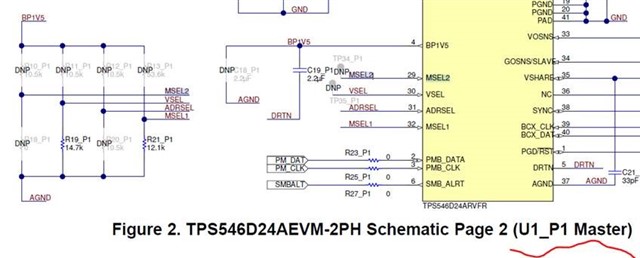
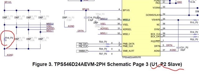
1. I think the schematic of the TPS546D24AEVM demo board has a problem. That is Master and Slave Config pin(MSEL2) are connected together.
This will make Master config affected by Slave, which makes Master MSEL2 is pulled to GND.
Does it make EVM be set to Standalone Mode(EVM datasheet table 7-11), not 2-Phase Mode?
But in this situation, I found that the EVM GUI tool can still read 0x0001 from ECh register, which means that the config is two-phase mode(EVM datasheet figure.7-87).
Does it relate to TI EVM NVM setting? If yes, I would like to know the NVM setting in TI EVM.
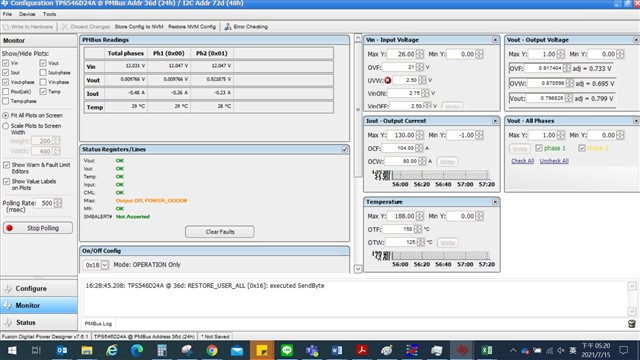
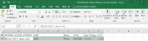
2. There is something wrong with the reading value on Iout(0x8C). Ex. The reading value on the TPS546D24A EVM GUI tool is 0xC4DD, and convert to Decimal is equal to -3.14A. But in reality, the value should not be negative. It should be 0xC4DD (Heximal)=11000 10011011101(Binary) =>1245*2^(-8)=4.86A。In addition, the current value=4.86A is weird,because there isn't any load on TI EVM output.
3. The voltage register reading value on Slave is not correct. We always read 0.92V on GUI, even we set 0x18 on 0x2 register to shut down O/P voltage. The GUI can still read 0.92V on Slave and the current value is also incorrect.