This thread has been locked.

If you have a related question, please click the "Ask a related question" button in the top right corner. The newly created question will be automatically linked to this question.

CSD18563Q5A: weak mechanical drawings

Part Number: CSD18563Q5A

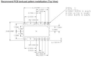
Systemic data sheet weakness.

Mechanical dimensions for footprints in most data sheets looks to be done by some mechanical engineers, or some summer interns. 

Assumptions and conventions from the mechanical engineering field correspond poorly to generating data for making foot prints in a EDA package.

Simply, a footprint drawing is not like any other mechanical drawing.

Needed:

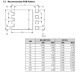
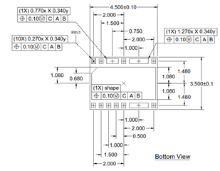
  • Center of each pad as an offset from the center of the part. Center, is the middle of the part where the part and place machine picks the part up.
  • Size of each pad. 
  • Pitch, i.e. distance from pad to pad in repeated patterns.

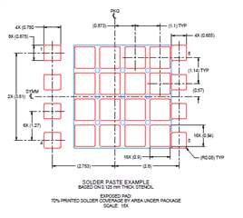
Stencil openings are usually defaulted to some value by EDA program, and do not need a separate drawing, unless a very large pad where it can be split up and/or reduced.

This may look totally "wrong" to a mechanical engineer, but this data is not being fed into a CNC machine or handed off to some machinist.

TI is not alone in this tradition of unsuitable information, which has a long history. 

Also, PDF's of TI data sheets are not name by their part number, which does not help. 
I gave give examples of competitors drawings and PDF's that are actually helpful.
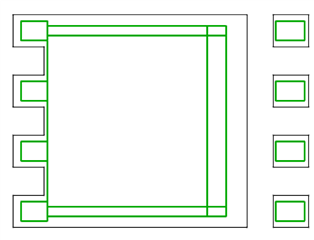
Good:

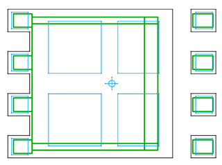
The foot print drawing was fuzzier 

https://www.qorvo.com/products/d/da005701

  • Hello Chris,

    Thank you for your interest in TI FETs. I apologize if our documentation does not meet your expectations. Have you taken a look at the CAD symbols available for this device? Below is a link for CAD/CAE symbols in the product folder found under Design & development. We support many popular formats. Please review and let me know if you require additional information.

    https://www.ti.com/product/CSD18563Q5A#design-development##cad-cae-symbols

    Best Regards,

    John Wallace

    TI FET Applications

  • I have not yet checked the dimension of that foot print against the drawing. It look reasonable.

    For giggles I took all the dimensions in the datasheet: package drawing, "PCB pattern" and Stencil opening into a CAD program.

    As the PCB pattern lacks any center point, which is included in the Q5A Package drawing and the Stencil opening, the center pad can be estimated. The package drawing has a center point but none of the dimensions are directly referenced to it.
    Layering the three drawing on top of each other shows a poor match between them. It may "work" but is sloppy workmanship.

    Green is the exposed metal on the part, not all pads are added. 
    Yellow is the max part outline.

    Violet is the suggested PCB pattern.
    Light blue is the stencil opening.

    Solder mask is missing altogether.

    Stencil opening extends beyond metal on part. 

    Footprint pads are shorter than the actual  part.

    This is what happens when you have bad drawings, too many numbers and only a few of them are relevant. 

  • Hi Chris,

    I have requested additional details from our packaging team and will update you as soon as I have more information.

    Thanks,

    John

  • The Library offered has problem, the center pad is made with polygons, it will make my program go crazy.
    Solder mask are also polygons, bad for the same reason. 
    The paste mask extends beyond the metal of the part, if the part drawing is correct.

    The thin yellow line on the left of "D" pad is the end of the drain metal.
    Solder mask openings have been rounded to make pasting operation easier. Sharp corners trap solder and makes stencil hard to clean.

  • Hello Chris,

    I received the updated and attached drawing. Let me know if I can be of further assistance.

    Best Regards,

    John

    DQJ0008A-datasheet.pdf

  • looks great! Thanks!

  • The updated package and footprint drawings have more detail, thanks. It includes some tolerances.

    In the above sketch with the new foot print and package dimensions,  I'm estimating the position of the package on the PCB 

    as it would float in reflow.

    Having stencil openings for the whole middle pad, as implied, would put to much solder on the pad (black lines) and lead to solder balling.

    The original stencil drawing would work if the maximum dimension in the indicated tolerances would be the case.

    Are those package tolerances real?

  • Hi Chris,

    Thanks again for your interest in TI FETs. Below is the feedback from our packaging engineer.

    Best Regards,

    John

    Page 4 of the package drawing is the stencil.

    The opening for the center pad is not in one piece.

    It was divided into multiple. (Red color)

    See below.


  • Yeah, I saw that. Its looks like the stencil openings cover non-solderable surfaces of the FET. 
    Is the mechanical drawing of the case correct?

  • Chris,

    Yes, the mechanical drawings of the package are correct.

    John

  • Hello,

    Then why would it be necessary to add solder to the non-solderable section of the package?


    Thanks

  • Chris,

    I checked again with the packaging engineer. His response is below. If you have additional questions or need more information, please email me directly at jwallaceri@ti.com

    Thanks,

    John

    The stencil was designed according to the PCB pad.

    The PCB pad are slightly larger than the component pad.

    This is to ensure that the component pad still making good
    contact with the PCB pad during reflow even if the package
    slightly shift or rotate.


    Pin 1-4 are relatively small compare with the thermal pad.

    This size difference can cause the package to shift or
    rotate during reflow.