This thread has been locked.

If you have a related question, please click the "Ask a related question" button in the top right corner. The newly created question will be automatically linked to this question.

[FAQ] Common land pattern for both UCC23513 and TLP5754

Part Number: UCC23513
Other Parts Discussed in Thread: UCC23313, UCC23511, UCC23313-Q1, , UCC23511-Q1,

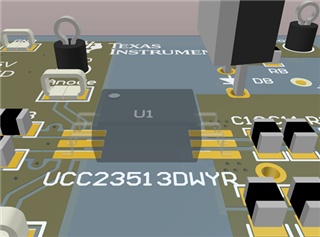
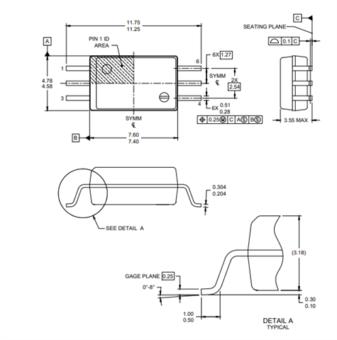
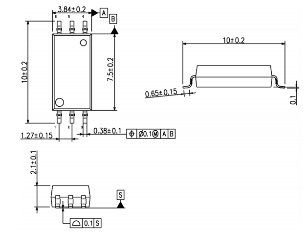
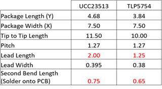
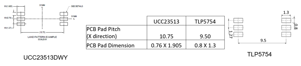
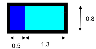
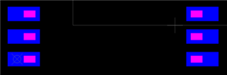
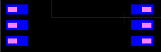
Is it possible to design a PCB land pattern to fit both the UCC23513 and the TLP5754?

(UCC23513-Q1, UCC23511, UCC23511-Q1, UCC23313, and UCC23313-Q1 all use the same package, so this FAQ applies to them as well)

  • Part Number: UCC23513

    The same package designator (SO-8, SO-6, SOIC) from different manufacturers may have slight variations in dimensions and recommended land patterns. It may be possible to design a common footprint that allows you to use similar parts from multiple suppliers giving you a better continuity of supply. Below is an example of a land pattern that can be placed on your PCB that will accept either the UCC23513 or the TLP5754.

    UCC23513DWY and TLP5754

    The body size is similar between these two devices, but the lead forming is different, resulting in different recommended PCB land patterns. Shown below in Figures 1 and 2 are the package outlines from the respective datasheets, and a comparison of the various dimensions.

                              Figure 1 - UCC23513DWY Package Outline

                                Figure 2 - TLP5754 Package Outline

                 Table 1 - Comparison of dimensions from package outlines

    While the body and the pin-to-pin pitch in y-direction are similarly sized between the two devices, the lead lengths are significantly different, resulting in different recommended PCB land patterns:

    This figure depicts an overlay of the two recommended land patterns:

    Green = TLP5754 PCB Pad

    Red = UCC23513 PCB Pad

    Yellow = Overlapped of two PCB land patterns

    Based on this, we simply extend the land patterns specified by TLP5754 datasheet 0.5 mm wider (depicted in dark blue) to accommodate either device:

    Light Blue = Original TLP5754 PCB land pattern

    Dark Blue = Proposed Extended PCB land pattern

    The PCB Pad Pitch in the x-direction increases to 10 mm in this revised land pattern.

    Comparing the two devices mounted on the same land pattern, first TLP5754:

    Blue = proposed PCB land pattern

    Dark pink = TLP5754 lead contact point

    And, when the UCC23513 is mounted on the proposed land pattern:

    Blue = Proposed PCB land pattern

    Light pink = UCC23513 lead contact point

    The pitch between land pattern in the y-direction remains 1.27 mm. There is no change to the spacing in the y-direction.

    You can see one land pattern design on your PCB can now accommodate either device.

    Subtle differences may occur due to solder paste formulation, thickness, etc, so please verify your design before sending it off to production.

    If you have any questions, please click the "Ask a related question" link above, and we will be happy to help you!

    Best regards,

    Don

    Isolated Gate Drivers Applications Engineer