This thread has been locked.

If you have a related question, please click the "Ask a related question" button in the top right corner. The newly created question will be automatically linked to this question.

UCC27212: The out put had pulse wave

Part Number: UCC27212
Other Parts Discussed in Thread: OPA455, SN6501

Hello, TI  Expert :

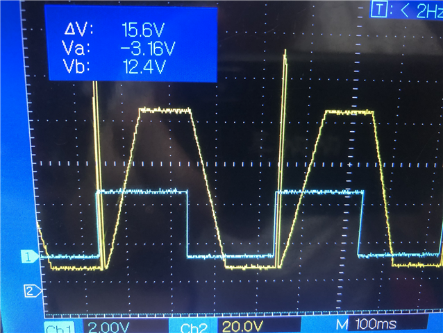
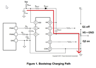
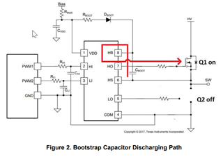
1.I am use UCC27212 to control the MOSFET on or off, but when I turn the high side MOSFET on, the HB PIN  will  occur pulse wave, I don’t  what is happen. Can you help to analyze ?

2.I try to change C8 to 0.5uF the pulse wave still exist. Also change C7 to 1uF.

below is the schematic 

01_source_0913.pdf

  • Hello,

    Thank you for your question. Could you please clarify exactly where in the circuit are you measuring the signals on channel 1 and channel 2 of the oscilloscope?

    What is the state of transistors Q1 and Q2 when LO and HO are switching?

    The high side driver on UCC27212 uses a bootstrap circuit to charge the bootstrap capacitor between HB and HS. During the low side ON state (LO = High, HO = Low) the bootstrap capacitor charges (see path on Figure 1 of application note below), so you need to have a path from HS to GND through the low side switch in order to charge the bootstrap capacitor. 

    Then during the high side ON state (HO = High, LO = Low) the charge on the capacitor is used to supply HO and turn on the high side FET (see Figure 2 of applications note below).

    Here is an applications note that describes the bootstrap circuit and how to select the components:  https://www.ti.com/lit/an/slua887/slua887.pdf?ts=1631554272309&ref_url=https%253A%252F%252Fwww.google.com%252F

    Regarding the capacitor values, please make sure VCC capacitor (C7)  is at least 10 times greater than the bootstrap capacitor (C8).

    Regards,

    Leslie

  • Hello Leslie 

     Sorry to make you confuse of the questions .

    1. The blue CH1 is measure U2-PIN7, The yellow CH2 is measure U2-PIN2 T1.

    2.What is the state of transistors Q1 and Q2 when LO and HO are switching?

    >>> When the HO = High, LO = Low the OPA455 will output the rising edge from 0V to 95V, When LO = High, HO = Low the OPA455 will output the falling edge from 95V to 0V.

    3. In this circuit  it had damage some  UCC27212, Can you help to point out the problem ?

    4.From the reference design https://www.ti.com/tool/TIDA-01418#tech-docs. should I add the diode to boost voltage? Should I add the resister at gate PIN of the MOSFET ?

  • Hi, 

    Thank you for the details.

    "When LO = High, HO = Low the OPA455 will output the falling edge from 95V to 0V" -> Does this mean that when LO=High and HO=Low, the Q1 and Q2 transistors are open? Therefore there is no connection between the high side Q1 source and the low side Q4 drain? The reason I ask is because, in order for the bootstrap circuit to work, the bootstrap capacitor must be charged and this done when the low side FET is ON to allow the charging path shown on the image below. But if Q2 and Q3 in your circuit are open when LO is high, then there is no path for the bootstrap circuit to recharge. 

    We usually recommend having a placeholder for a gate resistor in the board design to have the flexibility to add resistance if needed. The purpose of the gate resistors is to slow down the rise/fall time to limiting noise and ringing in the gate drive path.

    Regarding the diode, could you please clarify which diode you are referring to? 

    Best regards,

    Leslie

  • Hello Leslie

    1.could you please clarify which diode you are referring to? 

      >>> I think I get the wrong part number UCC27712QDRQ1. We are use UCC27212 that had include the diode in the chip.

    2.Does this mean that when LO=High and HO=Low, the Q1 and Q2 transistors are open? Therefore there is no connection between the high side Q1 source and the low side Q4 drain? .

      >>> I think the Q1 and Q2 transistors is control by the OPA455, so when  LO=High and HO=Lo Q1 and Q2 transistors are open. 

    3.Is there some other solution to achieve this function. When the capacitance charging the high side is ON and the low side is OFF, then capacitance is discharging the high side is OFF and the low side is ON.

  • Hello, 

    Thanks for the information. We typically don't see these Q1 and Q2 transistors added in the path between the high side and the low side switches. Could you please help me understand what is the purpose of this circuit with the amplifiers (OPA21921DGK and OPA455) and Q1/Q2 on your schematic?

    Regarding your question: "is there some other solution to achieve this function" Could you please clarify what function you are referring to? 

    Best regards,

    Leslie

  • Hello Leslie

    1. This is an other thread to talk about the OPA455 and Q1 Q2

    (+) OPA455: the current is step by step - Amplifiers forum - Amplifiers - TI E2E support forums

    (+) OPA455: how to increase output current - Amplifiers forum - Amplifiers - TI E2E support forums

    2. I just consider to make High side ON and the low side OFF to charge the capacitance, and high side OFF and the low side ON to discharge capacitance. Because the max frequence is 2.5Khz so it only use MOSFET instead of physical relay.

  • Hello,

    It looks like the circuit with the opamp and Q1 and Q2 is an emitter follower to have higher current gain from the signal from the op amp input. It seems the half bridge driver is being used to switch on the path to the Q1 collector and Q2 collector.

    The potential problem we see is that to charge the driver HB to HS capacitor there needs to be a path from the HS pin close to ground which normally occurs when the low side FET is turned on in a half bridge. With the with Q1 and Q2 in the path of the HS pin to ground I don't see how to have Q4 and Q1 and Q2 on to provide a path for the HS pin to switch close to ground which is required to charge the HB capacitor from VDD thru the internal boot diode in the driver.

    For this circuit, you may need to add a floating high side bias for the HB to HS capacitor charging. The SN6501 or SN6505 is a simple solution to provide this floating high side bias for the driver.

    Regards,