This thread has been locked.

If you have a related question, please click the "Ask a related question" button in the top right corner. The newly created question will be automatically linked to this question.

TPS54620: TPS54620

Part Number: TPS54620

Hi team,

Recently I 've been testing the TPS54620EVM and want to figure out the EC table specs . Here I have some confusion about the EC table specs shown in the section 6.5, page 6~7in the corresponding datasheet .

1. What does the error source/sink current mean ? How about the testing condition ?

in-phase end or out-phase end Current sourcing and sinking to the in-phase end ?

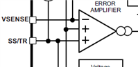
2.What does the ss/tr to Vsense matching means ?

3. Also I have some confusion about the FB resistors setting . Why larger resistors are required in order to improve the efficiency at light loads ?

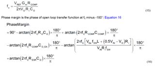
 I have read the technique article of "Loop Response Considerations in Peak Current Mode" ,as is said  , the worst phase margin happens at minimum Vin and minimum Io . However from the Phase Margin equation , the phase margin is independent of Io . Can you give me some guidance and advice ?

Thanks a lot for your support !

  • The application note can be reached by :https://www.ti.com/lit/pdf/slvae09

    Also, another question .Why should (Vin-Pvin)>4V if 100% duty is desired ,as is stated in page 21,above 7.4.4.

  • Hi Nini,

    Our US team will check then reply you soon.

  • Hi Nini,

    1. The error source/sink current shown under EC is the current expected to go through the error amplifier. The source current is the supplied current while the sink current is the received current, which I believe is out-phase meaning that they don't both occur at the same time. This device uses a transconductance error amplifier which compares VSENSE voltage to SS/TR voltage to Voltage Reference (usually 0.8V), which is a mechanism that minimizes output voltage overshoot, a type of output overvoltage protection (OVP).

    2. SS/TR to Vsense matching is compared by the error amplifier at startup of the device, used to regulate the output. This involves a series of comparison where switching is turned on/off according to the levels of this two pins, and Vref. When the device is turned on, SS/TRK voltage ramps up and creates a difference with Vsense voltage, this difference causes the Comp pin to also increase. When Vsense is greater than SS/TR, COMP goes down. When Vsense is less than SS/TR, COMP goes up. The COMP pin is compared to the switching threshold (0.25V), when Comp pin is bigger than the switching threshold, the High side MOSFET is starts switching. When Comp pin is less than switching threshold, the High side MOSFET is stops switching. The process repeats itself until Vout=Voutmin.

    3. Larger value resistors are required as they minimize the current going through the feedback divider. This current is in addition to the load, which means that for lower feedback-divider resistances, the power supply must provide more current and more power for the same load, therefore reducing efficiency. At light load currents, the differences in efficiency for different feedback resistances is more prominent as current through the divider dominates the current through the load.

    The following app note goes more into detail: /cfs-file/__key/communityserver-discussions-components-files/196/Design-considerations-for-a-resistive-feedback-divider-in-a-DCDC-converter.pdf 

    4. You can incorporate Io in the Phase Margin equation as it has Vo, so you can probably use the relationship of Vo=Io x Ro, rewritten as Io=Vo/Ro. You must know what Ro is in order for that relationship to work.

    5. The (Vin-Pvin)>4V if 100% duty statement normally applies when there's split input voltage rails. The nFET of the high side switch requires that the gate voltage be above the drain voltage for turn on. If VIN is separate from PVIN and VIN - PVIN > 4 V, then the BOOT charge can be constantly refreshed and true 100% duty cycle is possible. If VIN = PVIN, then quasi-100% duty cycle is possible, then the VIN min is 4.5 V, so the BOOT cap will always recharge to above the 2.1 V BOOT UVLO on each BOOT recharge cycle. When drop out conditions require that the on time be extended, the high side FET can stay on past the normal 100% duty cycle until the BOOT voltage falls below the BOOT UVLO. At that point, the high side switches off and the low sides switches on briefly to allow the BOOT cap to recharge. Then the high side will switch back on again and extended on time can resume until the next BOOT charge refresh is required.

    The following app note goes more into detail: https://www.ti.com/lit/an/slyt747/slyt747.pdf 

    Regards,

    Eileen Hernandez

  • Your explanation is so detailed !Thanks for your support and patient explanation , which definitely solved my confusion !

    Best regards !