Because of the Thanksgiving holiday in the U.S., TI E2E™ design support forum responses may be delayed from November 25 through December 2. Thank you for your patience.

This thread has been locked.

If you have a related question, please click the "Ask a related question" button in the top right corner. The newly created question will be automatically linked to this question.

TPS54308: circuit protect

Part Number: TPS54308

Hi Sir,

I now use tps54308. If the feedback phase compensation capacitor C6 is used on the designed substrate,
it is approximately more than 50pF,
Does the protection circuit work when the power is turned on? Unable to output normally.
Correctly, it is temporarily off after tens of pulses SW,
Send dozens of pulses off.
Please tell me the reason.

It seems to be turned off due to abnormal voltage detection of FB terminal.
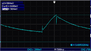
On DSO, it turns into a triangular waveform with a peak value of about 0.9V, so it seems to be protected.
Under this condition, when the DSO probe of FB terminal is equivalent to 1:1 and about 10PF is inserted between GND,
Because no delta voltage is generated and no protective measures are taken, I think C6 is carried out too much or the gain becomes high.
Therefore, I think the C6 value will change according to the pattern layout.
is it correct?
Thanks for your clarification.
Regards,

  • Hi ,

    what's the Vin-Vout-loading and LC config of your application ?

    C6 is the compensation circuit not a protection circuit . What do you mean with the ""protection circuit ?

    If the load transient meets the design requirement, no need to add this C6. 

    You can refer below file for details Optimizing Transient Response of Internally Compensated DC-DC Converters (Rev. B)

    BRs,

    Young 

  • Hi Young,

    I meant that whether the circuit triggers any protection caused by the value of C6.

    Thanks.

  • Hi Young,

    In the 5V output of 24V input, the average current in the load range is 0.1A ~ 2A,and the peak value is 3A.
    Digital equipment such as MCU and analog equipment are mixed, and the temperature range is 10 ℃ ~ 40 ℃, so the environment is "relaxed".
    Since C6 is 0 to 10 pF, the SW is intermittently causing ripple voltage to be 3 times or more.
    At present, it is planned to adjust R2 at about 30pF.
    Then the Loop gain is evaluated later.
    Thanks.

  • Hi,

    TPS54308 is a FCCM devices , which means that it will be forced into CCM even at light load. So the ripple would be same at all loading condition .

    C6 is related with the steady state performance , won't trigger any protection .

    if the ripple voltage to be 3 times or more, this circuit may be not stable at this moment . Could you help capture some waveform , SW, VOUT RIPPLE , and Inductor current if possible ?

    BRs,

    Young 

  • Hi Young,

    As you said, the state after L1 is unstable,
    It is considered that the decoupling capacitors C4 and C6 are not fully functional,
    Therefore, I found that ESR is very high and cannot be switched after checking C4 and C6, so I want to try to replace it with tantalum capacitor.
    The present situation is that the ripple is as high as 50mV, so we decided to take a look at the situation again.

  • Hi,

    Glad that you have ideas to figure out the reason , the Cout may be deceptive with the derated/effective value. You can try a MLCC cap then.

    To better understand this abnormal / unstable case, could you help share the latest BOM and SCH for us to check ?

    and If the C6 ESR is high , please help remove the C4 and try it again. 

    PS. Which pins are the attached waveform ? did you measure with the closest loop ?

    BRs,

    Young

  • Hi Young,

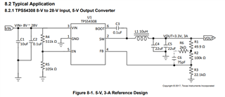
    The circuit is the same as figure 8-1 on page 13 of datasheet.

    The same reference numbers are C1 ~ C5, R1 and R6 are zero ohms, R2 is 100k, R3 is 15K, C6 is 40pF variable, and L1 is 15uH.


    C4 and C5 total 47uF, ESR 0.16 ohm (100kHz). In this state, the pulsating voltage is 100mV.

    TDK ceramic c4532x5r1e226m 250kA can be got tomorrow, so the test is carried out. Then I send the ripple.

    Thanks.

  • Hi Frank,

    Thanks a lot for sharing , it's much clear now. 

    Regarding the C6 cap, it is not needed when COUT has high ESR. 

    And you can refer chapter DS 8.2.3.5.3 Feed-Forward Capacitor to select a more reasonable cap .

    BRs,

    Young

  • Hi Young,

    Thank you.

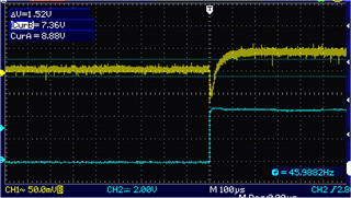
    Please find the ripple when the scheduled capacitor is attached.

    ripple2

    If there is no C6 equivalent, a wide step response DSO ripple is sent at 50 pF.

    No cap

    50pF


    I will measure Loop gain later.

    Thanks a lot.

    Regards,

  • Hi ,

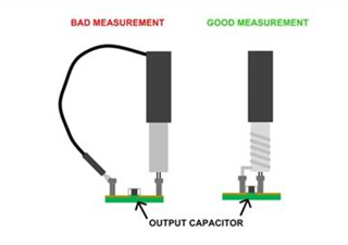
    For the ripple results, I'm good with it . Only one thing need to consider or double check is that suggest to measure the ripple with the closest loop as below .

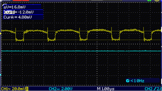
    For the 2nd and 3rd pic, form my understanding the yellow trace is the ac value of Vout, then what's the blue one ? and the loading is changing at this moment ?

    BRs,

    Young

  • Hi Young,

    On the part layout of the test PCB,
    L1 is close to C4 and C5, and DSO detection is connected near the capacitor terminal,
    a strange ripple is formed induced by L1, I'm very sorry.

    As speculated by the yellow line 1ch, the AC connection waveform of vout 5v line changes to 1A and 1.5A.
    This time, vout 5v and analog 5V power supplies are shared, and the load change timing of digital 5V system and sampling timing of 5V system are asynchronous,
    Therefore, it is still necessary to consider the value of C6.

    Thanks a lot.

    Regards,

  • Hi,

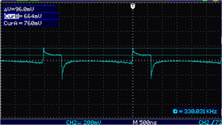
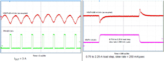
    For the Vout ripple , you can refer below left waveform with the closest loop .

    and you can also refer the load transient with the right waveform .

    for the "vout 5v and analog 5V power supplies are shared", what it means ?

    BRs,

    Young

  • Hi Young,

    Thank you for the attached picture.
    II use this device to convert from 24V to 5V and use it directly to the thermistor or the photocoupler LED side 5V.
    In addition, it is reduced to 3.3V from 5V to 5V digital device and series regulator, and it is supplied to RX72N and FPGA of Renesas.

  • Hi Frank,

    is it possible to talk offline , please share the real sch to my mail young-zhao@ti.com , you can mark the Vout 5V, analog 5V , digital 5V and system 5V in the sch? and how it is changing ? also i'm confused which rail is reduced to 3.3 V.

    BRS,

    Young

  • Hi Young,

    Thank you for your detailed explanation.

    We will start evaluating this IC.

    You can close this ticket.

    Thanks again.

  • Hi Frank,

    Sure, please let us know if there is any concern .

    BRs,

    Young