This thread has been locked.

If you have a related question, please click the "Ask a related question" button in the top right corner. The newly created question will be automatically linked to this question.

UCC28742: UCC28742DBVT

Part Number: UCC28742

Dear members,

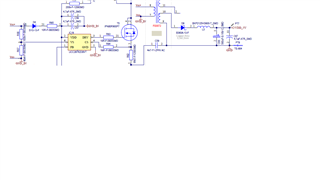
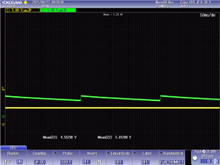
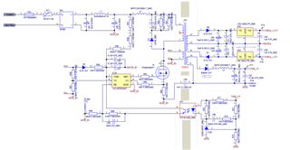
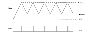
I have used the chip “UCC28742DBVT” for designing a Power supply and I had compared our design with the designing tool of TI too. But there is an issue that I can’t understand. In two samples of ours, the circuit behaviour is not as we expected. I tried to check the fault protection part. VDD and Vs aren’t the ones that I expected. All the other component values are as the same as other functioning boards.

At the beginning I thought that there might be an issue with VS because I can't see the designed value on it and subsequently the MOSFET connected to the board isnt functioning. I checked all the values, they are all OK and as same as the functioning boards. I couldnt simulate the circuit because there is no PSPICE model for simulation.

I appreciate it if somebody can help me on this.

Thanks in advance

Farzaneh 

  • Hello,

    You may be having an issue with a protection fault being triggered.

    The following application note describes the most common issues with fault sensing and how to resolve them.  I believe this application note will help you troubleshoot your issues.

    https://www.ti.com/lit/an/sluaac5/sluaac5.pdf

    Regards,

  • Thanks for your response. With the doc that you sent me I could verify the design values. But there is a problem. As you can see in the photo attached, I need to observe 5V at the test point7. 

    while I don't have any load at the output the signal is varing and it's not constant (green) and clean. but when I connect the load the signal stays at approx 4.5 (yellow)

    Is there any explication for that?

    Regards 

    Farzaneh 

  • Hello,

    The application note that was sent was to help you trouble shoot the design it it were shutting down do a fault, OVP, OCP or input UVLO.

    Could you probe the Aux, CS, VDD and Vout to make sure there was not a fault present?

    I reviewed the partial schematic you sent and you have the output rectifier D8 connect to L3.  This will create problems for you flyback design.  This is because when you discharge the energy in your flyback transformer to the secondary L3 will not react well fight the Instantaneous current. It will cause excessive voltage at the secondary.  I would recommend remove or L3 or put a capacitor from D8 cathode to ground.  A 270uF capacitor would do it. 

    Also the design needs some pre-load to keep it in regulation, I would recommend adding a resistor across the output.  2 mA of load should do it.

    Also this controller needs opto feedbeek to regulate the output as well.  Please refer to the data sheet and study the typical application schematic.

    Regards,

  • Dear Mike, 

    This is the whole design of mine and I have a load of 0.5 A  at the output. On one of the non- functioning board I could see that the MOSFET tries to switch but it's not able to that. I cheched the Vaux,CS,VDD and Vout, on the functioning one all are correct. on the broken board Vdrive isnt what I expected. I guess that there is a problem with Vout at start up. Still investigating....

    Regards

    Farzaneh

  • Hello,

    L2 will also give you issues.  I would recommend shorting that inductor out it is not needed.

    It sounds like you have a working board.  Study VDD, Vout, Aux and the CS on the working and none working design.  This should help to understand why the design is not regulating correctly

    Regards,

  • Hello Mike,

    Refering to the application note that you have sent me earlier, I could see that I have the same problem as it is mentioned on section 6. VDD looks like a saw tooth. Can you help me to understand why it appears? I can't find out why it happens, as I have functioning boards that have the same design, and they are working properly. 

    I can see these waveforms exactly.

    Regards

    Farzaneh

  • Hello,

    That waveform shows an input under voltage condition.  If VDD is cycling between VDD(off) and VDD(on) it indicates a fault.  

    The application note discusses how the input voltage is measured through the Vin/Vaux = Np/Na turns ratio.  It is looking for an IVSL(run) current greater than a certain value.  It should be listed in the UCC28742 data sheet.

    Did  you have a chance to read the application note through.  It goes through each fault and what causes the fault and how to remove them.  By probing the CS, Aux, VDD and Vout you should be able to determine which fault is preventing you from starting up and the application note should help you resolve it.

    Regards,

  • Dear Mike,

    I changed the chip and it works properly. I might damage the chip by soldering and desoldering a lot.

    Thanks for your support.

    Farzaneh