This thread has been locked.

If you have a related question, please click the "Ask a related question" button in the top right corner. The newly created question will be automatically linked to this question.

UCC27211: Unusually high spikes in SPICE simulation

Part Number: UCC27211

Hi Experts,

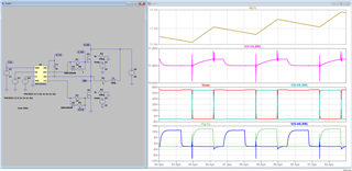
I'm simulating a half-bridge setup using UCC27211. For the FETs used, Cgs=4.7n, Cgd=1.8n, Cds=6.9n (all at VDS=0v). I'm observing unusually high spikes in Vgs-LS, Vgs-HS in LTSpice simulation. Following is the sch and waveforms

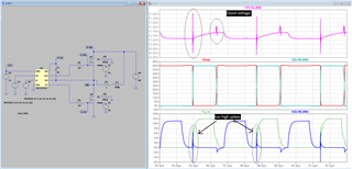
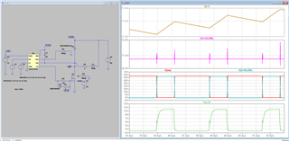
Load current is around 11.5A. I'm aware of miller effect but I dont think it'd be this severe. I connected a diode-resistor nw across 10ohm to provide a turn-off path. Following is the sch and waveforms of that -

The effect is still abnormal. The current is 11.5A here too.

Does this have something to do with the Spice model of UCC27211? What's causing the issue? Miller effect induced spikes shouldn't be this high, esp at the given voltage, current (60v, 11.5A). 

  • Hello Pranit,

    The Vboot voltage does not seem to have high spikes but the scale is expanded quite a bit. It looks like the  circuit is set up for a double pulse arrangement where the inductor is in parallel with the high side switch. Can you confirm the inductor current waveform in your sims?. Inductor current can reach very high levels in this configuration, and also the body diode of the MOSFET is force commutated which can result in high dI/dt and high dV/dt leading to high voltage spikes. I also see that the Cgd of 1.8nF is fairly high compared to Cgs of 4.7nF. There may be fairly high miller charge.

    Regards,

  • Yes the setup is a DPT but with 33% duty. The Qgd/Qgs-th ratio is 1.33 for the FET used in the simulation. I mentioned ~11.5A inductor current. Attaching a waveform of the same.

    As for the forced commutation of the HS diode, its a ZVS transition. There's deadtime bw HS, LS gate pulses, during which the HS-diode conducts. As for ind current commutation, from LS-MOSFET to HS-diode, its natural commutation. From HS-diode to HS-MOSFET, its forced commutation (near ZVS transition). dv/dt due to forced commutation is very small (dv=1.4v, dt=few ns). Effect of di/dt shouldn't be there because current is shifting internally from diode to MOSFET channel. Externally, there is continuous current between DS terminals. So, because of a continuous DS current, spikes across VDS shouldn't occur during forced commutation of the HS-diode.

    I replaced the HS MOSFET with schottky diode and ran the simulation. Following is the result - 

    The spike in VGS-LS during the start of plateau region is still there, although lower in amplitude. Could you verify the correctness of the SPICE model? And also check for any issues with the model, any cases where the math goes crazy and gives abnormal values?

    I'm attaching the model I'm usingUCC27211.LIB

  • Hello Pranit,

    Thank you for the update. I do see a significant difference in the waveforms in question with the last simulation with the schottky diode in place of the high side Mosfet. It looks like there could be significant impact from the FET switching characteristics, or one suggestion is to look at the deadtime of the LI and HI input signals. I would suggest increasing the dead time to 50ns, 100ns to see if you are seeing hard switching due to the timing of the low side and high side Fets during the Vds rising or falling times.

    We have run simulations at TI and supported customers with the UCC27211 model and have not seen abnormalities that were not expected due to power device switching characteristics or circuit parasitic elements included in the schematics.

    Regards,