This thread has been locked.

If you have a related question, please click the "Ask a related question" button in the top right corner. The newly created question will be automatically linked to this question.

TPS7H4001-SP: octal configuration

Part Number: TPS7H4001-SP

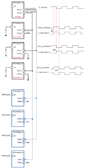
I have a question on the SYNC1/SYNC2 pins on the TPS7H4001-SP:  How many devices can these SYNC pins drive when operated in Primary Mode?

I’m considering operating 8 of these POLs either all individually, or in 4 groups of 2 in parallel, or in 2 groups of 4 in parallel.  I’m looking to have all POL devices synchronized to the primary device to avoid any undesired input “beat frequency” noise.  Leveraging Figure 7-6 from the datasheet, this would mean the SYNC pins wound need to drive upwards of 4 devices with 90° phase interleaving.  With no phase interleaving, the number of devices the SYNC pin would need to drive is 7.  I would like to know whether or not this is okay or if a buffer is needed.

  • Hi,

    We know from testing our 4-Channel EVM that one primary device can drive three secondary devices with no issues.  We have never tested driving more devices in parallel.  We believe the majority of capacitive loading is in the PCB routing as getting to seven other devices can be quite a distance to drive.  So this becomes highly dependent on your circuit layout.  I would suggest at a minimum, providing a placeholder for buffering of the clocks from the primary device.  You can bypass this buffering for initial testing to confirm there are no issues over your application requirements.  If issues are observed, then buffering can be used.

    Thanks

    Christian

  • Thanks Christian, I will advise the Team on this for their evaluation and testing. 

    However, is there a way for us to work with the design team to understand the drive strength of the Sync pin? the customer will for sure do some additional testing regardless but if we can provide some idea into the internal circuitry of the IC that would be helpful. 

  • I'll ask design team and get back to you.

    Thanks

    Christian

  • Thanks Christian, 

    any insight yet to the drive strength of the Sync Pin?

  • Hi Michael,

    Sorry for the delay.  It seems we don't have the resources to simulate this so my I recommend going with my first suggestion which is to make a place holder in layout for a clock buffer in the case issues are observed with driving multiple inputs.

    Thanks

    Christian

  • Thank you for following up Christian