This thread has been locked.

If you have a related question, please click the "Ask a related question" button in the top right corner. The newly created question will be automatically linked to this question.

BQ76925: BQ76925 Schematic Review

Part Number: BQ76925
Other Parts Discussed in Thread: BQ24115, MSP430G2553, TPS542951

Hello,

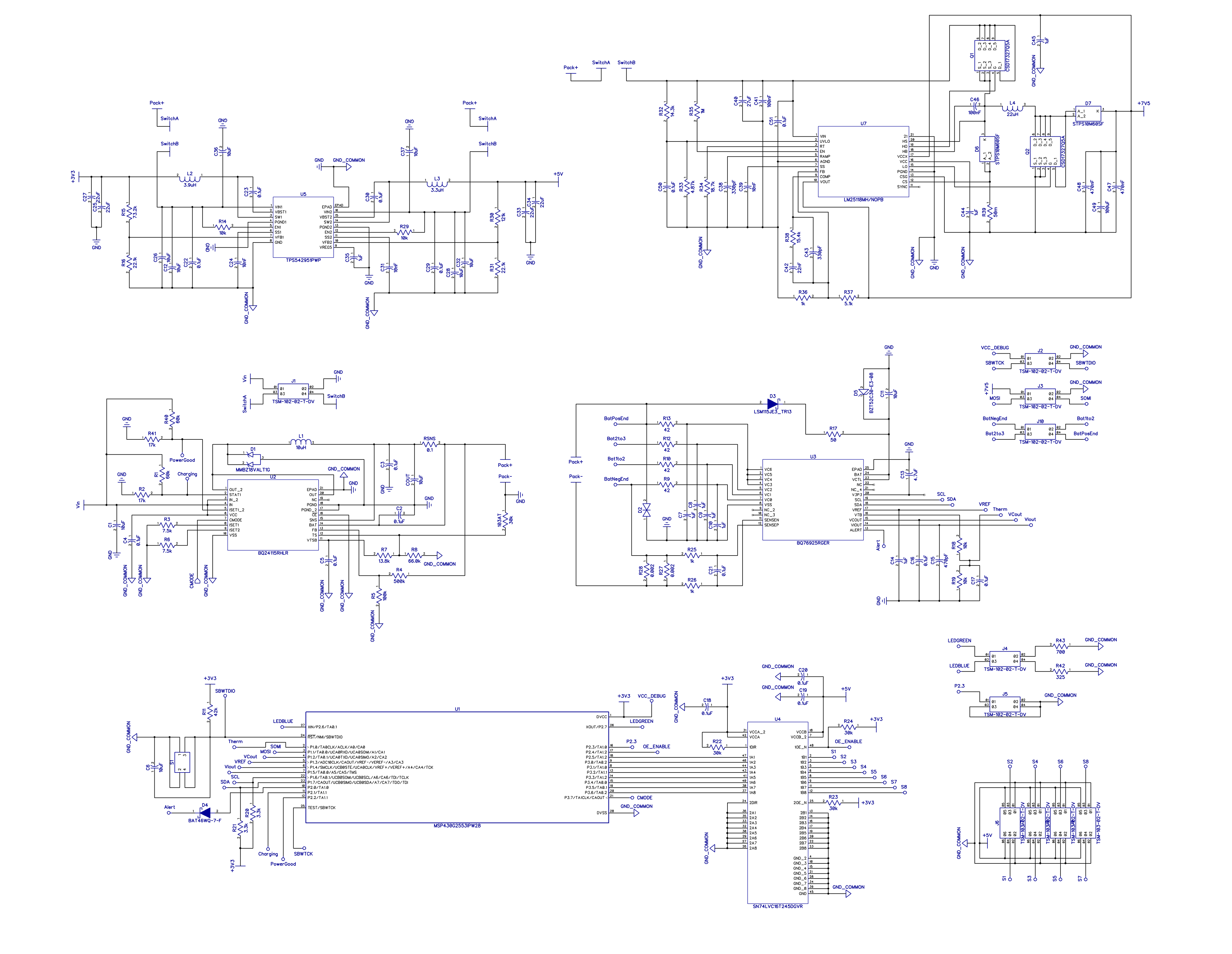
I was hoping for a review of my user of the BQ76925 in my schematic. It will be used in conjunction with the BQ24115 as can be seen in the schematic, it is intended to monitor the batteries, provide information about them, and rebalance the batteries as necessary. I was wondering if it would be better to have two different different BQ76925 ICs, as in (B) of the schematic image or if (A) from the schematic image would work just fine. Similarly the connection between the BQ76925 and the BQ24115 at Pack+ and Pack- is the intended setup between the two ICs, yes?

Link to Schematic

Link to Setup

Thanks you for the help

  • Hi Matthew,

    The schematic related to the BQ76925 looks basically correct. You have used single ended capacitors on the inputs, these give a well defined time constant to the filter but can be challenging to connect without exceeding abs max.  The differential filter capacitors shown in the data sheet 8.2 Functional Block Diagram, the EVM schematic, and the application note https://www.ti.com/lit/pdf/slua707  help maintain input voltages in range during connection.  I did not look at the other ICs extensively.

    The charger and battery monitor subsystems generally connect at the pack terminals yes, commonly there is a protection circuit between.  See the application note https://www.ti.com/lit/pdf/slua707 as an example where FETs are controlled by the MCU.

    Cells are commonly connected as diagram A where the cells are paralleled and act as a single cell with larger capacity with a single monitor.  Sometimes systems will want an architecture more like B with separate monitors, but it can be much more complicated.  If the system can disconnect one string the 2 parallel batteries can be at different voltages so some management must be done to avoid high current when the batteries are connected together.  If the 2 parallel batteries are not separated, when one cell is balanced it will pull current from the other string also.  

  • Thank you for the extensive reply, I looked into what you said and went over the schematic with that in mind. I setup the differential filter capacitors and added some protection circuits between components. Hopefully the changes I've made haven't created more issues to fix.

    The batteries will always be used in parallel with each other so differing voltages between the batteries shouldn't be a particularly large concern fortunately.

    I've attached the new schematic would you mind looking over the areas you noted for improvements?

    New Schematic

    Thank you for your time and assistance

  • Hi Matthew,

    I think the changes should work fine.  

    One thing I notice here and may have overlooked before is the grounding. In the BQ76925 data sheet the MCU is considered to reference the VSS of the IC so the single ended voltages measured are at the same potential.  These are in referenced to the battery- as shown in figure 8.  Communication with something referenced outside the sense resistor would have the communication lines modulated by the voltage across the sense resistor (pack current), and of course if the communication were to be referenced outside the FETs it would need some isolation or level shift.  The common referencing is also shown in the functional block diagram https://www.ti.com/document-viewer/BQ76925/datasheet/functional-block-diagram-slusam92733#SLUSAM92733 

    In your schematic you have the MCU and BQ76925 referenced with the charger on the pack side of the sense resistor.  SRP has the larger recommended range of the sense inputs,  so that connection will allow negative range of the input during discharge.  The BQ76925 does not have a polarity requirement, keep track of the polarity in your design.  The VC0 will also go negative during discharge which is not recommended. The cell 1 voltage appear lower during discharge in this condition.  See the note 2 in the abs max table https://www.ti.com/document-viewer/BQ76925/datasheet/absolute-maximum-ratings-slusam92186#SLUSAM92186 If the VC0 is driven sufficiently negative it may reset the part, the point at which that occurs is not characterized. In the common battery design this is most likely to happen with a sudden heavy load on the cells such as short circuit and differential capacitors connected to VC0.  This is the reason VC0 is filtered separately to GND in the functional block diagram.  

  • Thank you for the reply,

    I'm a little confused by the pack+ and pack- connection at the moment.

    If you look at Figure 17 in BQ241XX Datasheet you'll see that the BQ241xx device series has ground connected to the negative end of the pack, additionally the BQ24115 connects the the analog and digital grounds together through the pad on the bottom of the device, the digital ground that is also being shared by the MCU.

    This is where the issue occurs, firstly both BQ24115 and the BQ76925 need a common ground between them and the MSP430G2553, secondly, the BQ76925 expects that the ground is connected to the lowest point of the battery connection with Pack- separated by the Rsense resistor, yet the BQ24115 expects that the Pack- is connected to the ground, which connects to the MCU's ground, which as you see can't both be true, Pack- can't simultaneously exist at ground and also not at ground.

    So where should Pack- be?

    Do I need to connect BQ24115's Pack- to ground and have a 2nd Stage Pack-? But how would that even connect to any other parts?

    For example the TPS542951 is expecting that the power ground and the digital ground also connect through the EPAD of the device, does that imply that Pack- needs to be routed through a resistor at every other IC's GND as well? Does the BQ76925 even connect to the power ground (GND in the schematic) that the BQ24115 connects to or the digital ground (referred to as GND_COMMON)?

    Newest Schematic to Reference

    Thank you for the assistance and your time WM5295

  • Hi Matthew,

    Referencing circuits can be complicated, and you have a lot of questions embedded above.

    If you are going to sense current on the low side (which is the BQ76925 capability) you need 2 separate references or "grounds". With 2 references you need a method to signal between the references, or a part which tolerates voltages from the other reference, or can use the other reference, or accept the errors between.   Part of that decision is knowing the voltage difference between the 2 references. In this case the difference is created primarily by the sense resistor value and the battery current.  You will know how large the currents will be.   If the difference in the references is small, perhaps mV, this is likely easily accommodated in the noise margin of a digital interface. If the difference is in 100's of mV or V you likely need a special isolation circuit.

    One choice would be to ground everything at the PACK side of the sense resistor as you had before.  Again check the range of pins for damage and operation, as mentioned before the sense pin may be fine, VC0 won't want to measure below VSS so negative voltage would be lost and the bottom cell may look a little low.  If the negative voltage got too large it could reset the BQ76925.

    You want to measure voltages with respect to the VSS of the BQ76925 since it has single ended outputs with respect to its VSS.  If your MCU had differential inputs which could sense REF- and V- which tolerate the DC voltage, and the voltage across the sense resistor was within the tolerance of the I2C signals, you could operate the BQ76925 at BAT- and the remaining circuitry at the charger VSS/PGND.   The MCU shows a VREF- pin but I'm not sure you are able to use it that way.

    Another option would be to locate the MCU at the BQ76925 VSS at BAT-.  This way the BQ76925 keeps its input voltages in range of its VSS (except charge current).  The MCU's ADC references the VSS so it has the proper reference.  The charger will develop its voltage with respect to its PGND, that should go to the PACK-, the other side of the sense resistor from the BQ76925.    If the voltage reference is too large you might need to translate the control/status voltages from the MCU to the charger reference.  Power supply is also a consideration, you will know your architecture better.  In general most parts will tolerate some variation in the power supply voltage. If the variation is very dynamic or large you may need special consideration for referencing the supplies or isolating them also.

    So where should Pack- be?

    It must go to the charger reference.

    Do I need to connect BQ24115's Pack- to ground and have a 2nd Stage Pack-? But how would that even connect to any other parts?

    The BQ24115 will produce the voltage to charge the "battery", its reference needs to go to PACK-.  Generally you would be using the voltage from the battery outside the sense resistor which would be this reference potential also.  The MCU is likely an an exception since it seems to be single ended referenced to the BQ76925 outputs.  

    Pack- needs to be routed through a resistor at every other IC's GND as well?

    Not likely, they would seem to connect to the load of the "PACK" without need of current sense.

    Does the BQ76925 even connect to the power ground (GND in the schematic) that the BQ24115 connects to or the digital ground (referred to as GND_COMMON)?

    BQ76925 VSS seems best to be on the opposite side of the sense resistor.  See discussion above.

  • Thank you for all of your time and assistance with this design, I believe that this (hopefully) will be the last schematic. I took your above advice and separated the grounds, PGND (the power ground) connects with AGND (ground for the non-power ICs) under the BQ24115 as suggested by that documentation, meanwhile BGND will be separated from the rest of the devices only serving as ground for the BQ76925 and as the ADC voltage reference through the MSP430G2553's VREF- pin, which should be capable of accepting BGND as the negative end of the ADC measurement and VREF from the BQ76925 as the VREF+ for the MCU.

    Here is the schematic

  • Hi Matthew,

    Seems to make sense.  Hope it works well, let us know if you can.