This thread has been locked.

If you have a related question, please click the "Ask a related question" button in the top right corner. The newly created question will be automatically linked to this question.

LM5121-Q1: Can the location of the disconnect FET be moved before the current sense resistor

Part Number: LM5121-Q1
Other Parts Discussed in Thread: LM5121, LM2766

I would like to use the disconnect FET as an inrush limiter to the input capacitor.  That means that the FET would be before the input cap and the Vin/SCP connections.  Will this work or can it be made to work (with addtional circuitry)?  

  • Hi Dan,

    Thank you for considering the LM5121.  The answer is no, because the current sense amplifier as well as VIN pin must be energized before the disconnect FET is turned on.  You  cannot place CIN behind the disconnect FET either because it would affect the current sense signal.  If Vin/SCP is critical, you may consider to place two capacitors in series to protect against possible input capacitor short circuit fault, or use a quick fuse there.  

    Thanks,

    Youhao Xi, Applications Engineering.  

  • Thank you for the prompt response.  I should have been more clear in my description.


    I would plan to put a series resistor to pre-charge the input capacitor, so the IC would actually be powered, but not running because the UVLO will be held in the STANDBY state.  There will be an external uC that is monitoring many voltages and current, so the uC will know that the input cap has been charge up.  The IC will be powered but not drawing much current so the voltage drop across the pre-charge resistor will not  drop very much voltage.  I saw in the data sheet Figures 37 and 38 using the DG and DS pins to support an external FET for reverse battery protection.  I had not initially considered reverse battery protection, but that is an interesting addition.  Could Figure 38 be enhanced with an additional NMOS device to provide the reverse battery protection function and the inrush limiter bypass function.  R1 allows the input cap to charge at a reasonable rate (100 to 500 ohm resistor).  Then when the 5121 is ready to become active, the FETs would bypass the resistor and connect the cap to the input with about 5 to 10mOhm of on resistance.  There would be almost no voltage across the resistor when the FETs turn ON.   I realize that when the “disconnect function” is activated, that R1 will still keep some power to the IC, but with the external UVLO control, the device can be put in Standby or Shutdown.  Block diagram of the concept is shown below.  Would this work using Figure 38 as a starting point? 

  • Hi Dan,

    It is an interesting idea.  Figure 38 itself cannot be used as a inrush limiter because its body diode is pointing to the load side.  Your R1 will be bypassed by the body diode.  However, if you flip the NMOS, then it may work with R1 as an inrush current limit, but note that you lose the reverse polarity protection (because of be body diode pointing to the input source).  Anyway, we haven't tested such an inrush limiter circuit but I think you can test it to verify the functionality experimentally.  Experiment is always the necessary step.

    Thanks,

    Youhao

  • I was thinking of using a back to back FET to get the reverse battery protection and the inrush resistor bypass.  I believe that Drain on the first FET facing the input and Drain of the second FET facing the IC will do the trick.  I will add it in and test it.  Thanks.

  • Hi Dan,

    Thank you for verifying it.

  • I should have the prototypes in very shortly and will provide an update to this when they are in.

  • Thank you Dan.  We are looking forward to your good news. 

  • I am having trouble getting my Inrush/polarity protection circuit to function.   
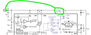
I realized that I needed to add a diode in series with the source (shown by the Green dot) to prevent the Gate-Source junction from breaking down (20V max).  I have verified that if I disconnect the Source from the 5121 and provide an external power supply to provide a -10V bias (Vgs) that the circuit will function properly.  I can turn both N-MOS FETs ON and OFF by controlling the P-MOS FET.  But even with the source disconnected from the 5121, the charge pump does not provide a positive voltage for the source.  I measure about 8 volts lower than Vin and I would expect it to be at least 10V above Vin.  I have connected a 100pF cap from DG to DS and a 499K resistor from DS to Ground as is shown in Figure 38 of the spec.  I am using the UVLO function to manage the inrush state.  I pull the UVLO to ground to put the 5121 in Shutdown mode while the inrush circuit allows the input caps to charge up through the polarity protection diode and the 499 ohm resistor.  Whe the system is ready to start the 5121, the ground is removed to allow the converter to start up.  (At least that was the plan)  But the charge pump is not doing what I thought it would do.  Can you see anything I am doing wrong?  

    Thanks.

  • Hi Dan,

    Thank you for your sharing. 

    Could you check the start up logical sequence?

    It should follow Figure 24 in DS. Where you device Vin pin and UVLO pin connector ? Is it Vin boost?  

    BR dehuan

  • Dehuan,  I will check the startup sequence, but I have done measurements with a volt meter and can verify that the UVLO voltage exceeds 1.2V and the VCC does turn ON.  I will try to get some scope curves of the sequence today and update this.  I have attached a schematic of the design for your reference.  This is a test board, so the sequence is started by me applying the external voltage (45 to 50V) with the P2 header connected to ground.  I have replaced diode D5 with a short so that the UVLO state is shutdown instead of standby.  This draws less power. I can see that the input capacitor charges up to a voltage that is close to the input voltage.  The R18 resistor does drop some voltage because the LM5121 draws some current while in shutdown.  Then I open up the ground connection on P2 to allow the converter to start up.  I can see that the input current increases, VCC turns ON, but the FETs do not turn OH and the voltage at the input caps drops because the increased current is still going through the R18 resistor.

    A few changes have been made to the values shown in the schematic.  R23 is now 20K to move the UVLO threshold to 30V, R22 is now 10K, C12 is now .033uF and the resistor connected to C5 was changed to 499K (my error when entering in the value during the initial design).  I have verified that the basic converter works.  I shorted across the Inrush FETs and removed the P-MOS FET Q3 and verified the basic design.  (P1 is connected to ground to provide the correct switching frequency)

    Page-1_LM5251-Design.pdf

  • As promised, here are some plots of the startup sequence.  I hope this helps.

    Scope_Plots_Startup.pdf

  • Hi Dan,

    This seems to be a very interesting phenomenon. It seems that there is a big drop in the Vin of the device,  DG pin is bias voltage of Vin voltage. The Vin pin voltage low than input voltage , so maybe the DG cannot turn on MOS.

    why the cap voltage droop so much? Is a load at boost output? or can you reduce  R18 value?

    BR Dehuan

  • I think I am going to abandon this idea for now.  I have other items within the power supply system to get running.  I was looking at using an external charge pump like the LM2766 (floating it from Vin to Vin-5) to create a "Vin + 5V" supply to turn on the P-MOS FET.  I have tested that if I put a positive voltage from an external supply on the P-MOS device it will turn on the P-MOS and then the N-MOS FETs.

  • Hi Dan,

    Thank you for your sharing. We can be communicated later if have any other idea.

    BR Dehuan