This thread has been locked.

If you have a related question, please click the "Ask a related question" button in the top right corner. The newly created question will be automatically linked to this question.

TPS650864: TPS6508641 - About OTP setting

Guru 21045 points
Part Number: TPS650864
Other Parts Discussed in Thread: TPS650861, BOOSTXL-TPS650861

Hi Daniel-san,


I understand that OTP of TPS6508641 is fixed by TI Factory.

Can I overwrite OTP of TPS6508641?

If I can overwrite, have two questions.


-------

[Q1]

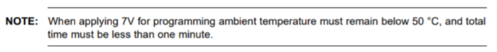
We refer to “TPS65086100 Non-Volatile Memory Programming Guide”.

Can this programming method be applied to TPS6508641?

-------


[Q2]

According to “TPS65086100 Non-Volatile Memory Programming Guide”,

“OTP bank can be changed from ‘0’ to ‘1’ but a ‘1’ cannot be changed back to a ‘0’”.


(Q2-1)

We guess that we can only overwrite "Bank1" once.

Is my understanding correct?


(Q2-2)

If we overwrite to Bank1, is Bank0 automatically deleted and Bank1 enabled?

-------


Regards,

Hide

  • Hi Hide-san,

    There are 2 banks of OTP on the TPS650864 devices. Bank 0 is pre-written but you can write to bank 1 following the method in TPS65086100 Non-Volatile Memory Programming Guide with the OTP generator

    https://www.ti.com/lit/pdf/swcu188

    https://www.ti.com/lit/zip/swca303

    You are correct that once OTP bits are written as 1 they cannot be changed back to 0. There is an OTP bit which determines the OTP bank to load from. So once bank 1 is written and this bit is set to 1 OTP bank 0 is not technically deleted but it will be inaccessible.

    Thanks,

    Daniel W

  • Hi Daniel-san,


    Thank you for the information.

    We have two questions.


    ---------

    [Q3]

    I understand that OTP bit of TPS6508641 is I2C address 0x38_Resister Address 0x03.

    Is my understanding correct?


    [From swca303]

    ---------


    [Q4]

    Currently, we supply to 7V to CTL4 pin but can’t confirm I2C address 0x38.

    And, we can’t find I2C address 0x38 in the TPS6508641 datasheet.

    Are the register configurations of TPS6508641 and " Table 5-64 of TPS650861" the same?


    Regards,

    Hide

  • Hi Hide,

    That is the correct address for the OTP bit.

    The I2C address should be 0x38 but will only be available during programming. The register configurations for both devices are the same.

    Thanks,

    Daniel W

  • Hi Daniel-san,

    Thank you for the information.

    Regards,

    Hide

  • Hi Daniel-san,


    We can confirm I2C address 0x5e but can’t confirm 0x38 on our board.

    So, we can’t write to PROGRAMMING_STATE.


    I have three questions.


    --------

    [Q1]

    Currently, we are setting up with the following steps.

    Could you please let us know if you have any concern?


    <Process>

    1. Powered on (VSYS=12V)
    2. Access to TPS6508641 by I2C.
    3. At the result, we can confirm I2C address 0x5e and can’t 0x38.
    4. Provide to 7V to CLT4 pin (CLT4 is pulled up to 3.3V by 10kohm)
    5. Again, access to TPS6508641 by I2C.
    6. At the result, we can confirm I2C address 0x5e and can’t 0x38.

    (By the way, we confirm all I2C slave address of bus line by i2cdetect command of Linux.)

    --------


    [Q2]

    I understand that the following comment at TPS65086100 Non-Volatile Memory Programming Guide, so “time must be less than one minute”.

    Could you please let us know the time if you have minimum total time?

    --------


    [Q3]

    Currently, we don’t use BOOSTXL-TPS650861 EVM.

    Is it possible to set OTP without EVM?

    --------


    Regards,

    Hide

  • Hi Hide-san,

    [Q3] it is possible to program the device without the board.

    [Q1] To access 0x38 please please refer to this excerpt from the programming guide: 

    "In order to access the registers in device address 0x38 the TPS65086100 must first be put into programming mode by writing the PROGRAMMING_STATE bit in the OTP_CTRL1 register to 1b. In order to access this register, 7V must be placed on the CTL4 pin. Once the PROGRAMMING_STATE bit in the OTP_CTRL1 register is set to 1b, remove the 7V from the CTRL4 pin. Once this is done all of the registers in the device can be accessed."

    [Q2] the minimum time for 7V to CTL4 will be the time it takes to write 1b to the OTP_CTRL1 register as stated above.

    Thanks,

    Daniel W

  • Hi Daniel-san,

    Thank you for the information and advice.

    Regards,

    Hide