


Hi Expert,
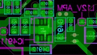
My customer is using tow TLV767-Q1 in the 12V->5V and 5V-3.3V. Here is the layout. They use the 4 layers board, and the picture is layer 4. The via is connected to layer 3 which is the ground plane.
Regarding to the thermal consideration, customer has questions below
1. Is that necessary to place the via under thermal pad? Or it's better route to GND_PIN then through via to layer 3?
2. As mentioned above, there are two TLV767-Q1. Do they need to route the GND of two devices to single via to avoid the noise? Or it is ok to have two via for each LDO to connect to ground plane (layer 3).
3. Is there any portion need to be modified in customer's current layout?
Thank you!
Pin
