Hi Sir,
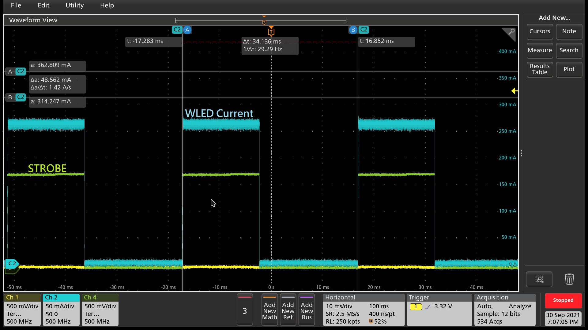
We used the WLED is made to flash by using an external STROBE as a trigger.
Among them, there is a PMIC in which current is flowing through the WLED without synchronizing with STROBE.
It seems that the internal LED driver is out of order.
Please tell us the possible causes.
We attached the schematic, WLED current waveform and STROBE waveform as below.
The schematic of OK module and NG module are the same.
Schematics: 2045.TPS68470_schematic.pdf
NG Module waveform:
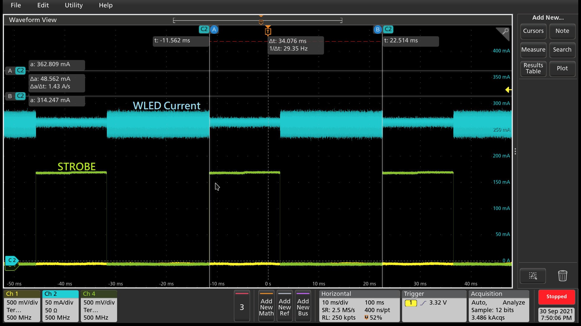
OK Module waveform: