This thread has been locked.

If you have a related question, please click the "Ask a related question" button in the top right corner. The newly created question will be automatically linked to this question.

LMR33630: based step-down converter burned occasionally -> new design

Part Number: LMR33630

Hi,

Harrison Overturf helped a lot in analyze what is the issue we are experiencing. That thread is locked, so I have to start a ne one. Here is the link to the original thread https://e2e.ti.com/support/power-management-group/power-management/f/power-management-forum/1031936/lmr33630-based-step-down-converter-burns-occasionally/3823571.

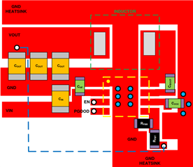
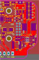
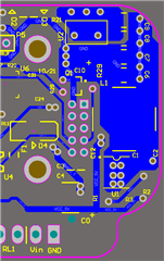
We have finished a redesign of the converter layout. It would be great if you could:

1. Please share your general thoughts if you see any potential issue in this layout, or if you have any additional recommendation.

2. We realized GND planes on input as suggested, but now there is a GND loop (marked with green line on the image) that could potentially act as antenna (we have a WiFi and RF antenna nearby). Do you see any issues there?

3. Should the input capacitors be connected with a solid plane, or to leave it as on image (marked with purple line)?

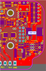
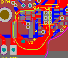
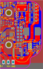
Here is the layout (Both layers, Top layer only, Bottom layer only):


Thank you,

Ivan Petrusevski

  • Hi Ivan,

    The layout looks good. In regards to the via, i would put more GND vias near the input ceramic capacitor to GND plane. How many layers is your board and what is your stackup?
    The high frequency loop will be in between the GND plane and the DAP of the IC

    Do you know where the regulation point for the converter is located? It is the top connection to R2 resistor. Normally we put this connection to the output capacitor. 

    Alternatively for cautionary purpose you may add a TVS clamp diode between VIN and GND to prevent excessive overvoltage near the connector. 


    Thanks

    -Arief

  • Hi Arief,

    Thank you for your reply.

    The board is a two layers, there is no dedicated GND plane. Only the top and bottom I shared in the original post. Since there is no GND plane, I do not have where to connect the GND vias on the input you suggested.

    There is a GND copper area in the bottom layer under the IC, and the thermal pad is connected to it with six vias.  

    R2 resistor is connected to the output voltage with the trace in the bottom layer. R2 is not close to the output capacitors, but that was realized according to the Layout example in the datasheet. Do you recommend that R2 should be closer to the output capacitors?


    What do you think regarding GND loop (marked with green line on the original image and on the image below) on the IC input? That was recommended in the original post, but my concern is if it could act as antenna (we have a WiFi and RF antenna nearby).

    Thank you,

    Ivan 

  • Hi Ivan,

    Sorry for the late reply. I missed this thread. In terms of your questions:

    1) R2 should be closer to the IC just like the recommended sample layout in the datasheet. 

    2) For the ground loop, i believe its ok. The important loop in on the ceramic capacitor C12, C3 and C4 since those are the high frequency filtering components. 

    Thank you

    -Arief

  • Hi Arief,

    R2 is already as close as it can to the IC, so I believe this is ok. Regarding the GND loop, I will break it so it it will not be a loop just in case. But still I will keep C12, C3 and C4 close to the IC.

    Thank you

    Ivan 

  • Hi Ivan,

    Thanks for the update, I'll go ahead and close this thread. If you have further questions related to this, feel free to open this thread again by posting a reply.

    Regards,

    Harrison Overturf