This thread has been locked.

If you have a related question, please click the "Ask a related question" button in the top right corner. The newly created question will be automatically linked to this question.

UCC21710-Q1: OUTH/OUTL Always gives -3volts

Part Number: UCC21710-Q1

These are the following Inputs/outputs we have given:

Inputs:

Pin 15 - Vcc  - 5V

Pin 9 - Gnd -  Gnd from supply

Pin 10 - IN+ - pulse from microcontroller

Pin 11 - IN-   - Gnd from microcontroller

Pin 14 - Reset - kept open

From separate DC DC converter

Pin 5 - VDD - 15V

Pin 3 - COM - gnd 

Pin 8 - VEE -   -3V

Pin 2 - OC - kept open

Pin 1 - AIN - kept open

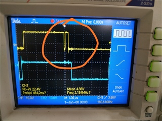
when we measure output between pin 3 and 4 we always see -3volts. can you please help us know if any incorrect or missing inputs? what could be the reason for voltage being clamped to VEE.?

  • Vamshi, 

    I strongly recommend to connect OC and AIN to COM pin if not being used. Especially OC, since leaving it floating can trigger short-circuit detection fault. 

    RST cannot be left floating. I am quite confident this is why you are seeing the output stay low.

    RST pin It has an internal pulldown and if you leave it floating it pulls LOW to GND and will keep driver's output LOW like you are seeing

    You can see the internal pulldowns/pullups in page 25 of datasheet -> https://www.ti.com/lit/ds/symlink/ucc21710-q1.pdf#page=25

    If you do not plan to use OC detection at all, or are just doing some testing now, you can connect RST pin to IN+ or tie it directly to VCC for the meantime, this will automatically reset faults which you wont have anyways. 

    In the final circuit, i recommend to connect this RST to microcontroller, depending on your design need/goal. 

    If this answers your question, please press the green button. 

    Best

    Dimitri

  • thank you for the reply.this does solve the issue but i have a question here...we are using UCC21710-Q1 as gate driver for a SIC-MOSFET  in a High frequency application(100KHZ) . When we tested this IC on bread board,we get correct pulses at pin 3 and pin 4( . But Same IC when used in the gate driver circuit ,pulses have notch at the end of each half cycle(photograph attached ). tested both at 20KHZ and 100KHZ.pulses when seen at pin 10,11(IN+,IN-) they are correct..

  • Hi Vamshi, 

    Sorry i didn't see this earlier. When you hit green button after replying, it moved the thread from closed to 

    Which signal is blue and yellow? These are measured at the GATE? the signal looks very clean and 

    I would like to ask to provide schematic and layout if available, along with the switch you are driving. 

    To me it looks like false turn-off but I dont see any big indication of large noise/EMI there. If this is being used in a larger circuit, I would ask you the question of what else is happening/ switching in the circuit at that time. 

    Due to the timescale and the fact that the output drops completely to VEE level, the device probably isn't tripping RDY or FLT signals, but still check those regardless at this time point. 

    Best

    Dimitri

  • hey...thanks for response.

    Actually I got the reason for it. This IC is not making any problem. I am using TI IC SN65116xE in between of microcontroller and gate driver IC. The output of SN65116xE IC itself has notches. Don't know what is the reason?

  • Vamshi,

    That is somewhat good to hear.

    If you need help with that part (differential receiver?), you can create a new thread for it. You can also try to add RC filter to sensitive inputs.

    I will close this thread. Reach out here or create new thread if you have any other questions.

    Best

    Dimitri