This thread has been locked.

If you have a related question, please click the "Ask a related question" button in the top right corner. The newly created question will be automatically linked to this question.

Vref Delta and Post Radiation Data

Part Number: LM117HVQML-SP

Hi, I am trying to understand the Delta and Post Radiation Data, in particular for Vref, for worst case tolerances of the output voltage.

The orderable device that we will be using is 5962R0722962VZA.

  1. For the post radiation, the max vref becomes 1.45V. How much of this change is seen immediately, so that we can compensate with altering the set resistor values?
  2. How do the Delta parameters play into this? 

For some additional context, the 1.45V is potentially introducing >+15% output voltage relative to the nominal 1.25V. This is a significant (and intolerable) amount of tolerance, and I am looking how to compensate out the error. Thank you.

  • Hi Steve,

    Thanks for reaching out. Here are a few answers I can provide:

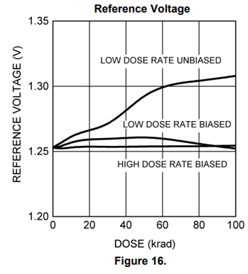
    1. The post-radiation min/max values in the datasheet are referring to Total Ionizing Dose (TID) radiation specifically. Since TID effects are accumulated over time, there is no large immediate change. However, you can see how much the typical reference voltage shifts across TID in Figure 16 from the datasheet. The orderable device you will be using (5962R0722962VZA) is rated for Low Dose Rate TID, which was accumulated at 10 mrad/s during testing. The time needed to accumulate a given level of TID can be calculated using the accumulation rate.

    2. The Delta parameters listed in the datasheet are meant to indicate parameter shift due to aging effects (Group C, life test). These values are measured at 25°C and do no include any radiation effects. 

    Hop

    Hope this helps.

    Thanks,

    Sarah

  • This is great, thank you so much Sarah! Yes, very helpful.

    I do have a few follow on questions.

    1. What is meant by the part being "biased?" We are using as in Figure 20.
    2. Does this part get any radiation testing/screening? If so, is there a section in the datasheet that indicates how the part characteristics may change due to the screening?
    3. The "typical" performance as shown in Figure 16 is drastically different from the 1.45V max provided in the datasheet tables (the table is much worse). Do you have any guidance how to reconcile the two? I am trying to do worst case tolerancing, which is difficult to do with figures using typical performance.
      1. I suspect part of the answer lies in how the device is used. For example, biased performs much better than unbiased; and perhaps the 1.45V is accounting for such configurations that make the tolerance worse.
      2. If this is true, I am wondering if you can provide any information about what causes the tolerance to go more in the direction of 1.45V, so I can see if they apply or not.

    Thanks,

    Steve

  • Hi Steve,


    Great, I’m glad this is helpful. Here are a few more comments on your follow-up questions:

    1. “Biased” means that the device is powered, whereas “unbiased” means that all of the pins are grounded to mimic being in a standby state. Both tests are performed to ensure that any susceptibility a technology may have to radiation under either condition is characterized. For this device, “biased” testing was done with VI=60V.

    .

    2. The electrical characteristics table is meant to provide a range of min/max values that each parameter will fall within, while the figures are meant to show how the typical value of a parameter will shift due to a particular variable (such as TID in Figure 16 or temperature in Figure 8). Each parameter in the table has a distribution curve of values that it may take, with the "typical" (or "nominal") value being most common and the mix/max values being cutoffs that are used during post-manufacturing screening of the parts. The min/max range from the table encompasses variation caused by part-to-part manufacturing differences, temperature (-55 °C to 125 °C, or subsets of this range as stated by the subgroups column), and any electrical conditions stated in the table’s test conditions. There is also some guardbanding added on top of this when determining the min/max range as a buffer to ensure that parameters fall within spec.

    As seen in the figure, the typical value of the reference voltage shifts with TID and thus the post-radiation maximum value given by the table also shifts in order to accommodate for the other sources of variation. As you noted, the worst-case shift occurs for this device when it is unbiased. Ensuring the device is biased would allow you to avoid the worst-case scenario for reference voltage shift caused by TID, but it is difficult to give an exact maximum value for this condition since the table only accounts for the worst-case (unbiased) scenario. An approximation could be made using the information from the figures and the conditions you expect for your application.

     . 

    I know this is a fairly wordy response, so please let me know if there is anything I can further clarify.


    Thanks,

    Sarah

  • Again yes this is very very helpful, thank you very much.

    The last remaining question: Does this part have an option for radiation screening, at which point we would receive parts that have already been exposed and the parameters altered? Is it tested biased or unbiased? 

  • Parts that are used for radiation testing are not sold. Regardless, parts that have been exposed and then removed from the source of radiation would go through an annealing process where the shifted parameters typically rebound over time. 

    I am checking with our radiation team to see if there is a TID report or other data available that would show the biased and unbiased reference voltage shift for a sample of devices. The actual drift is often much less than the min/max specs from the datasheet electrical characteristics table since the table is meant to encompass a much wider range of operating conditions. 

    I'll reply with an update once I hear back.

    Thanks,

    Sarah

  • Hi Steve,

    Here is the TID data for Vref provided by the radiation team. We are working on making the full report for this device available on its web page.

    For these tests Vref did not exceed 1.31842 V, which is well below the ensured datasheet maximum of 1.45 V. Hopefully this is helpful with regards to your reference voltage tolerance goals.

    VREF (V) - VDIFF=3V, IL=8MA
    Test Dose (krad) AVG MEDIAN MAX MIN SIGMA Upper Test Limit Lower Test Limit Median Delta (from 0 krad) Delta Ratio (to HDR) Max Unit Delta
    LDR - Biased 0 1.24822 1.24922 1.25046 1.23618 0.003555 1.3 1.2 0    
    LDR - Biased 3 1.24925 1.25056 1.25219 1.23835 0.00374 1.45 1.2    
    LDR - Biased 10 1.25179 1.25351 1.25571 1.24158 0.004073 1.45 1.2    
    LDR - Biased 30 1.25437 1.25562 1.25778 1.24632 0.003341 1.45 1.2    
    LDR - Biased 50 1.2541 1.25566 1.2618 1.24171 0.005753 1.45 1.2    
    LDR - Biased 80 1.24911 1.25097 1.25788 1.23671 0.005645 1.45 1.2    
    LDR - Biased 100 1.24562 1.24734 1.25422 1.23327 0.005563 1.45 1.2   1.81  
    LDR - Unbiased 0 1.24973 1.24984 1.25124 1.24727 0.000965 1.3 1.2 0    
    LDR - Unbiased 3 1.25149 1.25093 1.26155 1.24888 0.002922 1.45 1.2    
    LDR - Unbiased 10 1.25644 1.25562 1.26248 1.25395 0.002237 1.45 1.2    
    LDR - Unbiased 30 1.26463 1.26376 1.27423 1.25807 0.0043 1.45 1.2    
    LDR - Unbiased 50 1.28165 1.2799 1.28925 1.27601 0.003791 1.45 1.2    
    LDR - Unbiased 80 1.28973 1.28823 1.29832 1.28387 0.004288 1.45 1.2    
    LDR - Unbiased 100 1.29193 1.29103 1.30035 1.2847 0.00468 1.45 1.2 3.45 0.052
    HDR - Biased 0 1.24995 1.24984 1.25403 1.24657 0.001664 1.3 1.2 0    
    HDR - Biased 3 1.24916 1.24887 1.25366 1.24634 0.001669 1.45 1.2    
    HDR - Biased 10 1.24953 1.24947 1.25336 1.24587 0.001702 1.45 1.2    
    HDR - Biased 30 1.24935 1.24977 1.25386 1.24217 0.00258 1.45 1.2    
    HDR - Biased 50 1.2488 1.24996 1.25529 1.23615 0.004444 1.45 1.2    
    HDR - Biased 80 1.24792 1.24883 1.25672 1.23153 0.006186 1.45 1.2    
    HDR - Biased 100 1.24773 1.2488 1.25724 1.23016 0.006808 1.45 1.2      
    HDR - Unbiased 0 1.24969 1.24987 1.25216 1.24693 0.001419 1.3 1.2 0    
    HDR - Unbiased 3 1.24974 1.2499 1.25223 1.24698 0.001386 1.45 1.2    
    HDR - Unbiased 10 1.25008 1.25026 1.25261 1.24735 0.001375 1.45 1.2    
    HDR - Unbiased 30 1.25142 1.25154 1.2535 1.24926 0.001218 1.45 1.2    
    HDR - Unbiased 50 1.25428 1.25354 1.2564 1.2527 0.001327 1.45 1.2    
    HDR - Unbiased 80 1.25978 1.25918 1.26257 1.2572 0.001831 1.45 1.2    
    HDR - Unbiased 100 1.2623 1.2618 1.26509 1.25963 0.001709 1.45 1.2      

    VREF (V) - VDIFF=40 V, IL=8MA
    Test Dose (krad) AVG MEDIAN MAX MIN SIGMA Upper Test Limit Lower Test Limit Median Delta (from 0 krad) Delta Ratio (to HDR) Max Unit Delta
    LDR - Biased 0 1.25245 1.25296 1.25761 1.24381 0.003117 1.3 1.2 0    
    LDR - Biased 3 1.2535 1.25418 1.25601 1.24456 0.002874 1.45 1.2    
    LDR - Biased 10 1.25674 1.25795 1.26053 1.24777 0.003537 1.45 1.2    
    LDR - Biased 30 1.25961 1.26022 1.26286 1.25272 0.0029 1.45 1.2    
    LDR - Biased 50 1.26065 1.26189 1.26913 1.24895 0.005638 1.45 1.2    
    LDR - Biased 80 1.25579 1.25723 1.26547 1.24399 0.005624 1.45 1.2    
    LDR - Biased 100 1.25215 1.25383 1.26158 1.24037 0.005546 1.45 1.2   0.31  
    LDR - Unbiased 0 1.25306 1.2528 1.25807 1.25026 0.001695 1.3 1.2 0  
    LDR - Unbiased 3 1.2554 1.25427 1.27216 1.25255 0.004718 1.45 1.2    
    LDR - Unbiased 10 1.26122 1.26009 1.26859 1.25837 0.002639 1.45 1.2    
    LDR - Unbiased 30 1.27133 1.27012 1.28766 1.2632 0.006055 1.45 1.2    
    LDR - Unbiased 50 1.29232 1.28975 1.30157 1.28528 0.005129 1.45 1.2    
    LDR - Unbiased 80 1.30415 1.30424 1.31473 1.29627 0.005209 1.45 1.2    
    LDR - Unbiased 100 1.30792 1.30564 1.31842 1.29997 0.005543 1.45 1.2   2.97 0.067
    HDR - Biased 0 1.25299 1.25268 1.25716 1.2496 0.001686 1.3 1.2 0    
    HDR - Biased 3 1.25238 1.25204 1.25675 1.24961 0.001651 1.45 1.2    
    HDR - Biased 10 1.25295 1.25282 1.25682 1.2494 0.001676 1.45 1.2    
    HDR - Biased 30 1.25347 1.25389 1.25813 1.24617 0.002615 1.45 1.2    
    HDR - Biased 50 1.25372 1.2548 1.26068 1.24068 0.004621 1.45 1.2    
    HDR - Biased 80 1.25394 1.25496 1.26333 1.23695 0.006455 1.45 1.2    
    HDR - Biased 100 1.25439 1.25552 1.26441 1.2362 0.007101 1.45 1.2      
    HDR - Unbiased 0 1.25265 1.25273 1.25514 1.2499 0.001422 1.3 1.2 0  
    HDR - Unbiased 3 1.25265 1.25273 1.25514 1.2499 0.001422 1.45 1.2    
    HDR - Unbiased 10 1.25341 1.25361 1.25575 1.2508 0.00132 1.45 1.2    
    HDR - Unbiased 30 1.25554 1.25559 1.25758 1.25361 0.001196 1.45 1.2    
    HDR - Unbiased 50 1.25947 1.2588 1.26192 1.25792 0.001501 1.45 1.2    
    HDR - Unbiased 80 1.26674 1.26639 1.27035 1.26331 0.002269 1.45 1.2    
    HDR - Unbiased 100 1.27032 1.27052 1.27341 1.26678 0.002146 1.45 1.2      

    For the bias tests, the input pin was held at 15 V, while the output and adjust pins were connected through resistors to -15 V so that the load current was minimized to prevent internal heating of the device and possible self annealing. For the unbiased condition, all pins were grounded.

    HDR for these tests: 34-39 rad(Si)/s

    LDR for these tests: 10 mrad(Si)/s

    Sample size: LDR biased testing used 15 devices, LDR unbiased testing used 15 devices, HDR biased testing used 18 devices, and HDR unbiased testing used 15 devices. 

    Thanks,

    Sarah

  • Thank you, great info