This thread has been locked.

If you have a related question, please click the "Ask a related question" button in the top right corner. The newly created question will be automatically linked to this question.

ISO5852S: Power supply connection

Part Number: ISO5852S
Other Parts Discussed in Thread: UCC14240-Q1, SN6505B

Hi,

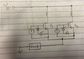
I want to use two ISO5852S ICs to drive two SiC MOSFETs in two parallel branches with common source (drain is not common). The MOSFETs will be used as high-side switches for my application. I have following questions regarding the bias supplies for the two MOSFETs.

1. Can I use a common power supply for the control sides of both ICs? In this scenario, both ICs will share a common control ground (GND1).

2. Can I use a common power supply for positive bias (VCC2) for both ICs? In this scenario, both ICs will share a common power ground (GND2).

3. Can I use a common power supply for negative bias (VEE2) for both ICs? In this scenario, both ICs will share a common power ground (GND2).

4. Will there be any potential problem (e.g., ground loop, shorting, etc.) that may arise related to ground reference? I am under the impression that all the power supplies are in some way are connected to earth ground and will it be a issue for ground loop/shorting?

  • Jonathan,

    Could you share a sketch of how the SiCFET's sources would be connected, or describe it?

    E.g.

    1) Each pair of SiCFET sources are connected to each other, but all 4 aren't. E.g. the first pair connected together and sourcing to one load, second pair sources connected to source to a different load. (2 loads / outputs of the HSS)

    2) All Four sicfets sources are connected together, and there (only 1 load/output of the highside switch. )

    3) All sicfet sources are independent (4 different outputs / loads).

    Best

    Dimitri

  • Hi Dimitri,

    Thanks for the response. A sketch is attached for reference.

  • Jonathan, 

    I'm assuming these are both N-ch SiCFET ( source arrow makes it look like a P-ch FET)

    In this case, you can use the same bias supply for both ICs. Since both sources are tied together, the reference from which we generated VCC2 and VEE2 for both gate drivers would be exactly the same. 

    In fact, you can probably use just one IC to drive both gates in parallel, but this depends on whether you need to switch the HSS at higher frequencies. 

    Often times HSS just needs to turn on with a very low frequency, so you could potentially drive them in parallel with the one driver if you can accept a slower turnon/turnoff. 

    If this answers your questions, please let me know by pressing the green button. 

    Best

    DImitri

  • Dimitri,

    Thanks for the reply. You're right, these are N-ch FETs. Let me know what you think about the biasing of the control side (VCC1). Will it be a problem if we drive both the ICs using a common DC supply? Is there any possibility of creating a ground loop due to common earth ground of the DC power supplies (VCC1, VCC2)?

    I am planning to use two ICs with different gating signals which are not synchronized in time.

  • Let me know what you think about the biasing of the control side (VCC1). Will it be a problem if we drive both the ICs using a common DC supply?

    Thats no problem and the norm. 

    Ground loop on the primary side is of little concern as you will have a ground plane on bottom layer or layer 2 depending on how many layers your PCB.

    Is there any possibility of creating a ground loop due to common earth ground of the DC power supplies (VCC1, VCC2)?

    You can create ground loops whether you use 2 bias supplies or not.

    You just need to have a good, uninterrupted ground plane/pour (source connection) on an inner layer. 

    I am planning to use two ICs with different gating signals which are not synchronized in time

    Even so, as long as the sources/GND2 reference is the same, you can use a single bias supply for both ICs. 

    If this answers your questions, please let me know by pressing the green button. 


    Best

    Dimitri

  • Dimitri,

    Thanks for your response. Would you suggest two separated ground planes (one for GND1, and the other for GND2) in the PCB design for high frequency operation?

  • You cannot connect GND1 and GND2 unless its on the low side, and even then you wouldn't want to connect them except for very simple testing as you essentially would just nulled the isolation and open up risks of electric shock etc. 

    If you need reference for schematic/layout I suggest to look at some of our reference designs, we supply the full design files for each as well.

    https://www.ti.com/product/ISO5852S#reference-designs

    The design for your switches would be very similar to any of the Highside drivers in these designs. For bias supply, I am not sure if you have already selected a part, but I would suggest to take a look at SN6505b / UCC14240-Q1 (very cool part, but 24VIN required)

    If you'd like us to review your design once completed we can also do that. Just open a new thread then. 

    If this answers your questions, please let me know by pressing the green button. 

    Best

    Dimitri

  • Dimitri,

    Thanks for the reply. Actually, by mentioning two separate planes for two grounds I was referring to design decision whether it will be worth a lot to have ground plane for GND1 instead of traces. I understand that connecting two grounds actually defeats the whole purpose of using the isolated gate driver IC in the first place.

    Thanks for suggesting the bias supply option. I will look into it.

  • Thanks for the reply. Actually, by mentioning two separate planes for two grounds I was referring to design decision whether it will be worth a lot to have ground plane for GND1 instead of traces. I understand that connecting two grounds actually defeats the whole purpose of using the isolated gate driver IC in the first place.

    I misunderstood your meaning, sorry about that. Thanks for clarifying.

    Actually, by mentioning two separate planes for two grounds I was referring to design decision whether it will be worth a lot to have ground plane for GND1 instead of trace

    You could probably get away with traces for GND1 but there are a lot of components (filter caps, bypass caps, etc) that need to connect to GND1 so its better to have a plane for it.

    Best


    DImitri