This thread has been locked.

If you have a related question, please click the "Ask a related question" button in the top right corner. The newly created question will be automatically linked to this question.

UCC256403: VCC and burst mode

Part Number: UCC256403

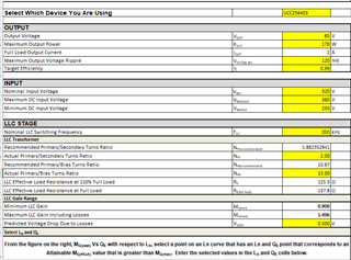
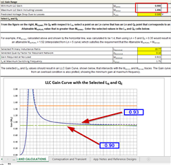
We follow your recommendation and move to the UCC256403 (https://e2e.ti.com/support/power-management-group/power-management/f/power-management-forum/1042317/ucc256303-skipping-pulses?tisearch=e2e-quicksearch&keymatch=ucc256303). Please, refer to that thread for more details about our application and specs (VIN = 240...380V, VOUT = 85V, POUT,MAX = 600W, option 3 selected on BW pin). 

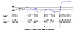
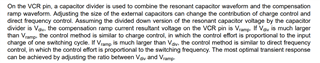
At fixed input voltage and load, converter enters burst mode when VCC > 16.5V. Scope acquisition below for 170W output power and 330V input voltage. 


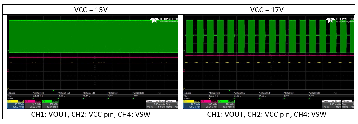
What might the reason behind that behaviour and how to avoid it? From the datasheet, I can see that VCC supplies the current generator of feedback pin.
But I didn't expect supply voltage to affect the overall feedback chain.


The same burts mode happens (at VCC = 15V) also if bulk voltage goes above 340V.

Kind regards

  • Hi Francesco,

    BW pin sets the BMTH/BMTL ratio where as LL/SS pin sets the BMTH Value. VCC value does not impact these burst mode thresholds. I am suspecting that BMTH value is higher. That could be the reason, the converter going into burst mode at 170W. Could you please share the design calculator (https://www.ti.com/lit/zip/sluc675) that you used for designing your converter using UCC256403. It would help me to debug. 

    Regards

    Manikanta P

  • Sure, please find schematic and worksheet attached.

    UCC256403 TI Design.xlsx

  • Hi Francesco,

    Thanks for sharing the design file. 

    After reviewing your design file, I identified that your power stage gain is less than the maximum gain required. Could you re-verify your design. Could you also re-upload the schematic as the uploaded one was not clear.

    Regards

    Manikanta P

  • Thanks for your reply.

    That's true at full-load. But - correct me if I am wrong- that should not be an issue at 170W (see graph below).

    We moved to lower gain during bench testing, as at certain point we thought that maybe too much gain in the resonant tank was the reason behind the high input voltage issue. Such as that even at the maximum achievable switching frequency, the gain of thank is too large for the controller to regulate the required output voltage and that would cause skipping pulses.
    So, we deliberately design a resonant tank with lower gain in order to verify that assumption. As that tank design did not fix the issue, the problem should be somewhere else.

    While debugging, we also find out that the same anomalous behavior was triggered by an higher VCC voltage. Thinking that it might be a clue of something wrong in our design, we asked for your help to sort it out.

    I hope this explanation makes sense to you. See also if the attached schematic is now more readable.

    Regards

    8686.sch.pdf

  • Hi Francesco,

    Burst packets due to change in VCC voltage:

    BMTH threshold is determined by the RVCC voltage and the LL/SS pin resistors (Please refer section 8.2.2.19 of the data sheet). I am suspecting that when you change VCC voltage, RVCC voltage is getting changed which would change the BMTH value. Could you sense this RVCC value for different VCC voltages. 

    Burst packets due to change in input voltage:

    When you increase the input voltage from 330V to 340V when VCC=15V, I would expect FBreplica signal to further reduce. I am suspecting that this FBreplica signal less than BMTL threshold. So, you are seeing the Burst packets. 

    You can try following steps to avoid burst mode at 170W:

    a.  you could try reducing BMTH threshold voltage by changing LL/SS pin resistors. Also, at the same time you can reduce the BMTL/BMTH ratio by changing BW pin resistor values. 

    b. You can also try disabling the burst mode by changing BW effective resistor value to option 7. In this case both BMTH and BMTL are set to 0.2V. In this case, If the feedback replica is less than 0.2V, for a long time, output voltage wont be regulated. However, if it is more than 0.2V, there shouldn't be an issue at all.

    I would like to address an issue when you design the converter at 600W but your actual operating power is at 170W.

    1. VCR pin signal is the control feedback for this controller. Here, VCR capacitors are designed assuming LLC operates at 600W. However, when you operate at 170W, VCR signal magnitude will be less. Due to this, controller operates more in direct frequency control rather than the charge control.

    Regards

    Manikanta P

  • Hi Manikanta

    thanks for your in-depth explanation.

    Burst packets due to change in VCC voltage:

    I can confirm that RVCC voltage is moving with VCC (when converter is switching).


    Burst packets due to change in input voltage:

    Losing regulation and audible noise are our main issues.

    a. We tried reducing BMTH threshold (and BMTH/BMTL ratio) to its minimum but the issue was still there.

    b. Even with option 7 selected the result was the same. How can i guarantee that feedback replica is never lower than 0.2V for a log time?

    Final operating power would be around 600W. So far, we tested this design up to about 450W.
    As I mentioned in the previous post, we are in the current configuration only to get a better understanding of that problem.
    Once we find out how to improve our design to fix it, plan is to move back to the original resonant tank that allows sufficient gain to achieve 600W.

    VCR:
    Capacitor divider will be changed accordingly.
    If i got the design procedure right, VCR capacitors are designed assuming nominal output power (to ensure maximum pin voltage and voltage swing on that pin is within limits). On a wide load range, VCR magnitude will can vary significantly. When light loaded, controller would operate more in direct frequency control rather than the charge control, if compared with heavy load behavior. 

    kind regards

  • Hi Francesco,

    Ideally RVCC voltage should be constant. I just realized that you were using very less capacitance at RVCC pin. It should be at least 5 times Boot capacitance. Could you check whether it solves the issue.

    Regards

    Manikanta P

  • Thanks for noticing that.

    Changing boot capacitance indeed solved the issue related to VCC voltage variation. RVCC is kept at regulated value of 13V

    Burst packets due to change in input voltage are still an issue.

    Regards

  • Hi Francesco,

    Could you send me the waveforms of low side gate signals for the different input voltages (at 320, 330,340) at 170W.  I would like to see the frequency at which converter is being operated. 

    I suspect that your converter is operating at high frequency region. At this high frequency, since the LLC gain is flat, Fbreplica signal should decrease. Can you share the FB pin voltage as well to see whether opto coupler is getting saturated during the burst mode. 

    Regards

    Manikanta P

  • Hi Manikanta,

    please, find the requested waveforms over a wide input voltage range (from 300V up to 350V).

    Regards

    waveforms_170W.pdf

  • Hi Francesco,

    Thanks for sharing the waveforms. I could see that when you increase the input voltage, opto-coupler is getting saturated which means feedback is working as expected.

    However the data that you shared is not consistent. That's because when the voltage is 320V, frequency is 148khz where as for 330V, frequency is 123kHz. Ideally this frequency should further increase. Also for higher voltages, I couldn't find whether the converter is operating in burst mode because time scale is too large.

    Since FB pin voltage is constant, could you remove the c15 capacitor which is connected across opto coupler. This capacitor should not be connected.

    So this time could you share following waveforms for all the input voltages:

    Set 1:

    1. SW node voltage (Zoomed in version to find the frequency of operation) - with frequency measurement

    2. VCR signal (please make sure peak to peak voltage less than 4.5V, If it's not within this range, increase lower Vcr capacitor value. see whether this solves the issue)- pk to pk voltage measurement

    3. output voltage- mean value measurement

    4. LO side gate signals - frequency measurement (I am asking both SW node voltage and LO gate signals because I do see a inconsistent pulse pattern)

    Set 2:

    1. SW node voltage (Zoom in such a way that burst operation is identifiable )

    2. VCR signal (please make sure peak to peak voltage less than 4.5V, If it's not within this range, increase lower Vcr capacitor value. see whether this solves the issue)- pk to pk votage measurement

    3. output voltage- mean value measurement

    4.LO side gate signals - frequency measurement (I am asking both SW node voltage and LO gate signals because I do see a inconsistent pulse pattern)

    I am assuming you changed the RVCC capacitor value as suggested before doing above measurements.

    Could you also let me know what option you are using for burst mode. And what resistances values you are using at BW and LL/SS pin to set the BMTH and BMTL threshold values?

    Regards

    Manikanta P

  • Hi Francesco,

    When I changed output power value to the 170 W in your design calculator to see the gain value in the high frequency region, I realized that gain value in the high frequency region is 0.93 where as required minimum gain is 0.9.

    This would definitely let the system work in burst mode when the input voltage is increased.

    Regards

    Manikanta P

  • Thanks Manikanta

    So we can rule out an instability issue of some sort. It is a inherent behavior dictated by the design choices.
    We noticed that the transition between the two operating modes happens when converter works beyond resonant frequency (gain < 1 ). Maybe it is just because the system has already reached the minimum available gain as you explained, and we should not worry about that if we choose a different combination of the resonant elements.

    I guess your suggestion would be to redesign the tank and to manage in a better way the trade off between the maximum required gain (at heavy load) and the minimum gain available in the high frequency region. Eventually we have to accept operating in burst mode at high input voltage and light load, if we still want to get maximum output power at low input line.

    Regards

    Francesco


  • Hi Francesco,

    You are absolutely correct. Also, please make sure below guidelines are followed while redesigning the tank.

    You can find these design guidelines in the following link: Designing an LLC Resonant Half-Bridge Power Converter Article

    Please let me know if you have any further questions.

    Regards

    Manikanta P

  • Thanks for your support.

    Kind regards