This thread has been locked.

If you have a related question, please click the "Ask a related question" button in the top right corner. The newly created question will be automatically linked to this question.

TPS7A3401: TPS7A3401 thermal issue

Part Number: TPS7A3401

Hi,

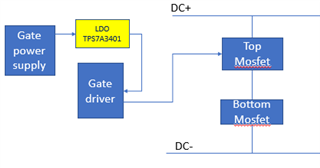
We are using TPS7A3401DGNR in our design for providing the negative supply to the gate driver IC.

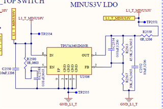
Attached the schematic reference of the LDO 

Regards

Smitha M S

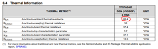
The maximum temperature as per the calculation is around 100°C, considering the following specifications

  • Input voltage = -11V
  • Load current (continuous) = 85mA
  • Output voltage = -4.8V
  • Rthja = 63.4 K/W


But with the actual measurement the temperature is going beyond 100°C with increasing the DC bus voltage (>650V)

Could you please confirm whether the Rthja value provided in the datasheet is with bare footprint or with some copper area.

Also please suggest if there are any other recommendation or modification with respect to existing design is required


  • Hello Smitha,

                          The θJA value presumes that the part is soldered on a JEDEC standard High K layout board which has no metal plane on the top layer of the board and only has some traces and the part footprint on the top layer. Could you clarify the following for me:

    (a) The specifications and the schematic have different VIN/VOUT conditions. Is this intentional?

    (b) The schematic component selections look fine to me. Could you confirm if the ambient temperature is 25°C?

    (c) If the Ambient Temperature is 25°C, the Junction Temperature TJ from the specifications provided would be TJ = TA + θJA*PD = 25 + (11 - 4.8)*0.085*63.4 =  60°C. Hence, it is not clear to me how the maximum temperature of 100°C was calculated.

    (d) When you say that the actual temperature is going beyond 100°C, are you referring to the junction temperature? If so, how is this being measured? Also where is the DC bus voltage being applied?

    Thanks!

    Regards,

    Srikanth

  • Hi Srikanth,

    Below is the response

    (a) The specifications and the schematic have different VIN/VOUT conditions. Is this intentional? 

    Yes since we were observing the heating issue we have tried reducing the voltage. Hence it is different

    (b) The schematic component selections look fine to me. Could you confirm if the ambient temperature is 25°C?

    Yes the ambient temperature is 25C itself.

    (c) If the Ambient Temperature is 25°C, the Junction Temperature TJ from the specifications provided would be TJ = TA + θJA*PD = 25 + (11 - 4.8)*0.085*63.4 =  60°C. Hence, it is not clear to me how the maximum temperature of 100°C was calculated.

    The calculation is for worst case ambient of 70C, but we are observing the above temperature at the ambient itself

    (d) When you say that the actual temperature is going beyond 100°C, are you referring to the junction temperature? If so, how is this being measured? Also where is the DC bus voltage being applied?

    The temperature is being measured on the case itself. Measured with thermal camera.

    DC bus voltage is applied to the Mosfet module and the LDO is used to give the required current for negative gate supply.

    Also please confirm whether the θJA value of 63.4 is without any additional copper area for the LDO.

    Regards

    Smitha M S

  • Hi Smitha,

                     The θJA value was calculated for a JEDEC standard board that does not have additional copper area on the top layer. Please note that θJA is very sensitive to the layout of the board on which the part is mounted. ΨJT and ΨJB are less sensitive to the layout of board, they could also be used to calculate the junction temperature (described on Section 10.4 of the datasheet). Thanks!

    Regards,

    Srikanth