This thread has been locked.

If you have a related question, please click the "Ask a related question" button in the top right corner. The newly created question will be automatically linked to this question.

TPS7A4701-EP: TPS7A4701,TPS7A33

Part Number: TPS7A4701-EP
Other Parts Discussed in Thread: TPS7A33, LMZ31704, LM27762, TPS7A39, TPS65131, TPS7A91, TPS7A47, TPS7A52, LM27761

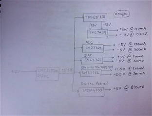
I am designing a power supply circuitry for the analog front end of my isolated data acquisition module.

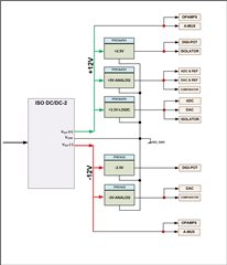
  1. The inputs are isolated +12V and -12V from an isolated DC/DC convertor
  2. The supply voltages required are +5V,+2.5V,+3.3V and -5V,-2.5V
  3. I am planning to use TPS7A4701 and TPS7A33 for generating various positive and negative voltages
  4. The planned configuration is attached here with
  5. As per the datasheet (SBVS204F:page-20) ,the power dissipation is "Power dissipation in the regulator depends on the input to output voltage difference and load conditions. PD can
    be calculated using Equation 7 .
  6. So my question is whether TPS7A4701 / TPS7A33 can be used for generating voltages,when the difference between input(12V/-12V) and required output voltages(+5v,+3.3V,+2.5V) are high

Just adding one more point: all output voltages have load requirements of around 700mA

Regards,

Chandru

  • Hi Chandru, 

    If you plan to have 700mA flowing then it will be difficult for many of these LDOs to remain within the specified temperature of 125C and will likely go into thermal shutdown. These device have a Rja thermal resistance of ~35C/W so that means the junction will heat 35C above the ambient temperature for every Watt dissipated. So generally I would recommend not dissipating more than ~2W. 

    You can improve the thermal dissipation with improved PCB layout (the thermal numbers in the datasheet assume a JEDED high-K board is being used, which is good but not great for thermal dissipation). We published an app note on how different board layouts affect thermal dissipation which can be very helpful in understanding the practical differences of various PCB layout techniques, in it you will see that you can improve the JEDEC thermal dissipation by 35%-50%. https://www.ti.com/lit/an/slvae85/slvae85.pdf

    You may want to consider having another DC/DC that drops the 12V to 6V or 7V in order to do so more efficiently and then using the LDOs for the final conversions. 

  • Thanks a lot for your reply.

    I have requirements of +12V,+5V,+2.5V (Positive rail) and -12V,-5V,-2.5V (Negative rail). Can you kindly suggest the topology,I can use for my requirements?

    The current requirements are as given below

    +12V @ 100mA

    +5V @ 500mA

    +2.5V @ 500mA

    -12V @ 100mA

    -5V @ 50mA

    -2.5V @ 60mA

    Option:1 ->  Use +5V  input (output of  a DC/DC) and derive all required supplies (including positive and negative rails)

    option:2 -> Use +5V  input (output of  a DC/DC) and derive positive  supplies and -5V  input (output of  a DC/DC) and derive negative supplies

    Can you please guide me how to derive negative supplies?

  • Hi Chandru, 

    You could use a Boost Converter to generate both the positive and negative rails. Here is an app note which covers the concept: https://www.ti.com/lit/an/slvaej3/slvaej3.pdf

  • Hai Kyle,

    Thanks a lot for your reply

  • Dear Kyle,

    I changed my topology and is as given below

    1. The input supply is +12V @ 2A
    2. Use the DC/DC Convertor (LMZ31704) to generate +5.5V
    3. Use LM27762 for generating ±5V @200mA and ±2.5V @200mA from the input +5.5V
    4. Use TPS65131 for generating ±13V . Connect to the LDO (TPS7A39) and generate ±12V
    5. Use LDO TPS7A4700 for generating +5V @ 800mA

    Attached with the topology. Can you please check and confirm,whether this is ok? In-case if the proposed topology is an over-kill,can you suggest any optimizations? 

  • Dear Kyle,

    Refer the new topology attached below.

    I am planning to use  

    1. LM27762 for generating ±5V @200mA and ±2.5V @200mA 
    2.  LDO TPS7A4700 for generating +5V @ 800mA

    What is the minimum input voltage to be fed? Can i use 5V as input for generating 5V output? or a minimum head-room is required between input and output?If so what is the minimum head-room between input and output?

  • Hi Chandru, 

    Regarding your question about  the minimum head room of LM27762, this seems ok to me but I'm going to loop in the Buck Switching Regulator team who support this specific product to make sure that is the case. 

    But generally, I think this topology makes sense due to your need for many plus/minus rails (+-12V, +-5V, +-2.5V). However I'm not sure how much noise the loads like the DAC can accept on its supply rails (especially around the switching frequency of the charge pump) and I'm unsure what the noise from the LM27762 will be at those frequencies. So if you don't already have a noise requirement for your rails, it would be good to know what they require and make sure you can meet those needs. 

    One thing I would note is that since you have reduced the input voltage going to the TPS7A47, you may not need a device with such a high input voltage. The devices that you may want to consider are TPS7A52 and TPS7A91, these are lower input voltage devices with very similar noise performance to TPS7A47, but come in MUCH smaller packages since they use lower voltage FETs. Below is a quick spec comparison and the PSRR plots which show the most similar conditions (changing the output voltage won't make a large difference given the same headroom). 

    TPS7A47

    TPS7A52

    TPS7A91

  • Thanks a lot for your reply. I will study about the noise requirements for the DAC and will revert back to you.

    Thanks again

  • Hi Chandru,

    I had a look on the headroom required for the LM27762. The positive output rail just has an LDO between input and output pins. This LDO has a dropout voltage of 95mV at 200mA of current. The negative rail has a charge pump and then and LDO between input and output pins. So here you should consider the output resistance of the charge pump + the LDO dropout voltage. For 200mA of load current, the charge pump output resistance is around 2.2Ohm. This would mean a drop of around 440mV on the charge pump. The dropout of the negative LDO is around 65mV. So in total this would be slightly over 500mV.

    Is the 200mA load a constant load in the application?

    Best regards,

    Varun

  • Hi Varun,

    Thanks a lot for your reply.

    The peak load is expected to be around 200mA and continous load may be around 150mA.

    Thanks & Regards,

  • Hi Chandru,

    Would the extra voltage drop of ~ 10mV at peak load be alright for the application? On the low voltage side (<6V VIN), LM27761 is the only regulated charge pump available that can support 200mA current.

    Best regards,

    Varun

  • Hi,

    Thanks for the inputs.I will check regarding the extra voltage drop of ~ 10mV at peak load

    Regards

  • Hi Chandru,

    Do you have any updates here? Do you need any further support?

    Best regards,

    Varun